↓
 

Robust Circuit Design

Exploring the design space

  • Home
  • Blog
  • Downloads & Articles
  • Products
    • Signal Wave Explorer
    • Signal Chain Explorer
  • Store
    • Shop
    • Cart
    • Checkout
    • My Account
  • Contact
  • About
Home→Blog - Page 3 << 1 2 3 4 >>

Post navigation

← Older posts
Newer posts →

Understanding SCE Thermal Noise Charts

Robust Circuit Design Posted on August 25, 2016 by adminAugust 25, 2016

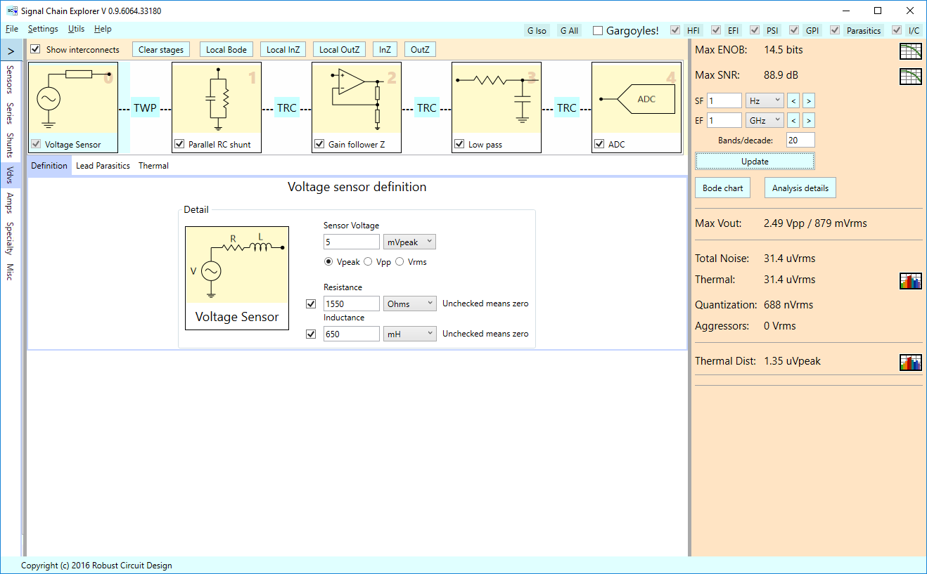
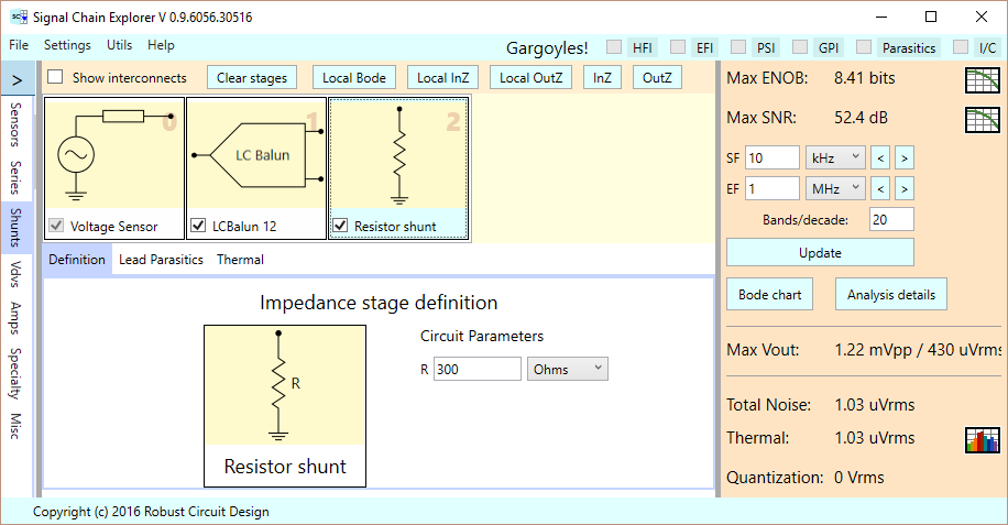
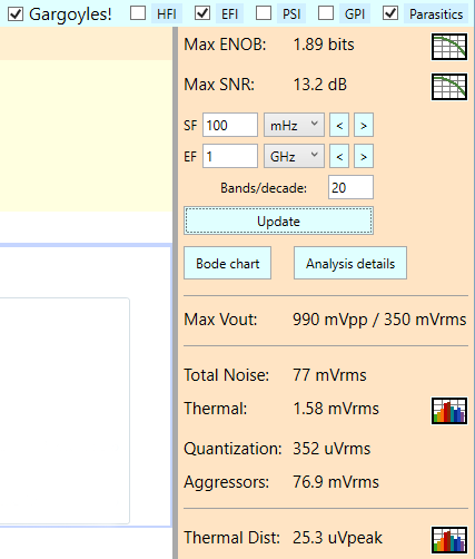
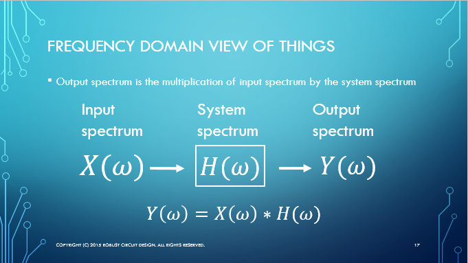
A key feature of Signal Chain Explorer (SCE) is its built-in ability to calculate and display the thermal noise in your signal chain. In this article, we take a look at thermal noise and how it is modeled and displayed in SCE.

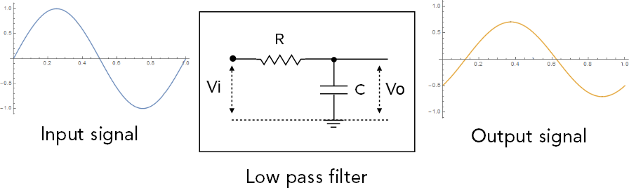
Thermal noise, aka Johnson or Nyquist noise comes about via random electron fluctuations which increase with the ambient temperature of your circuit components. All resistors exhibit this noise, which is Gaussian in nature, and this noise is deemed white, meaning it is present at all frequencies. Thermal noise is modeled in SCE by introducing an RMS error voltage associated with each resistor in the signal chain. For example, consider a simple resistive voltage divider, as shown below:

VDV with noise II

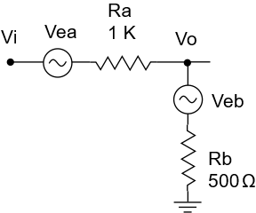
For each resistor, we add an error voltage in series with that resistor. Here, there are two error voltages Vea and Veb, which correspond to the resistors Ra and Rb, respectively. These error voltages can be calculated using the following well-known formula:

\(\displaystyle {{V}_{{noise}}}=\sqrt{{4KTBR}}\ {{V}_{{rms}}}\)

where K is Boltman’s constant, equal roughly to \(\displaystyle 1.38\times {{10}^{{-23}}}\), T is the ambient temperature in degrees Kelvin, often specified as 290 degK in most back-of-the-envelope calculations (and the default in SCE), B is the bandwidth of interest, in Hz, and R is the resistance in Ohms. Note that the resulting error voltage is Gaussian in nature, and we represent it as having units of Vrms.

Often, the thermal error voltage is specified in terms of a 1 Hz bandwidth, and the result is called the noise voltage density, with units \(\displaystyle {{V}_{{rms}}}/\sqrt{{Hz}}\). The noise density formula is:

\(\displaystyle {{V}_{{noise\ density}}}=\sqrt{{4KTR}}\)

The actual bandwidth is accounted for later by multiplying the noise density by the square root of that bandwidth:

\(\displaystyle {{V}_{{noise}}}={{V}_{{noise\ density}}}\times \sqrt{B}\)

Suppose our two resistances are 1000 Ohms and 500 Ohms, respectively. Then their thermal noise densities at a room temperature of 290 degK can be computed as:

\(\displaystyle Ve{{a}_{{noise\ density}}}=\sqrt{{4\times 1.38\times {{{10}}^{{-23}}}\times 290\times 1000}}=4\ nV/\sqrt{{Hz}}\)

and

\(\displaystyle Ve{{b}_{{noise\ density}}}=\sqrt{{4\times 1.38\times {{{10}}^{{-23}}}\times 290\times 500}}=2.83\ nV/\sqrt{{Hz}}\)

By the way, the 1000 Ohm resistor thermal noise calculation leads to a useful rule of thumb to remember when calculating thermal noise in your head:

\(\displaystyle 1000\ Ohms\Rightarrow 4\ nV/\sqrt{{Hz}}\)

Another useful rule of thumb:

\(\displaystyle 50\ Ohms\Rightarrow 1\ nV/\sqrt{{Hz}}\)

In order to incorporate thermal noise into SNR calculations, we must refer the noises to output. For our simple voltage dividers, the two error voltages referred to output using the voltage divider ratio:

\(\displaystyle Ve{{a}_{{rto}}}=Vea\times Rb/(Ra+Rb)=Vea\times 500/(1000+500)=Vea\times 0.3333\)

\(\displaystyle Ve{{b}_{{rto}}}=Vea\times Ra/(Ra+Rb)=Veb\times 1000/(1000+500)=Veb\times 0.6666\)

Now we can compute the thermal noise voltage densities of each resistor, referred to output, by using the numbers for the Vea and Veb noise densities calculated earlier:

\(\displaystyle Ve{{a}_{{rto\ density}}}=4\,nV/\sqrt{{Hz}}\times 0.3333=1.3333\ nV/\sqrt{{Hz}}\)

\(\displaystyle Ve{{b}_{{rto\ density}}}=2.83\,nV/\sqrt{{Hz}}\times 0.6666=1.8867\ nV/\sqrt{{Hz}}\)

SCE takes noise density calculations such as these and “sweeps” across the frequencies of interest in your simulation to produce a thermal noise chart. The figure below shows a (purposely coarse) thermal noise chart for our voltage divider example:

2016-08-24

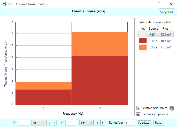
In this example, we are inspecting the thermal noise in the range of 1 Hz to 10 Hz. In computing thermal noise, SCE splits the specified frequency range into a series of bands, where each band is a chunk of the frequency spectrum. In our example here, we have two bands, one centered at 1 Hz, the other centered at 10 Hz. SCE computes the bandwidth of each band when computing thermal noise, and these bandwidths increase logarithmically with respect to the center frequency of the band. That’s because the thermal noise chart is logarithmic in nature. And it should be pointed out that each center point frequency is centered logarithmically in the band. To see this, below we’ve annotated the thermal noise chart to show the actual frequencies covered in each band of our example:

Annotated noise chart

In our thermal noise chart, we’ve chosen a chart resolution of 1 band per decade. So we have a band centered at 1 Hz, the other at 10 Hz. If we chose a wider frequency range, say to 100 Hz, we’d see a band centered at 100 Hz, and so on. Also, we usually use a much higher resolution than one band per decade. The default is 20, and it’s not uncommon to choose a 100 bands per decade, or higher.

In our example, the first band, centered at 1 Hz, covers the frequencies from 0.316 Hz to 3.16 Hz. The second band, centered at 10 Hz, covers the frequencies from 3.16 Hz to 31.6 Hz. Note that the blue labels shown circled with ovals above do not normally appear on the thermal noise charts — only the center frequencies are labeled for real. We’ve shown the band edge frequencies here to help you see the range the bands really cover. Yes, this a bit confusing, and we here at RCD are currently re-evaluating this design choice. But do note that normally you use a much finer resolution in the charts, so the actual bandwidths are a lot smaller and this detail becomes less important, and if we included the band edge frequencies, the labels would in general become too cluttered.

Okay, let’s put our knowledge of the band frequencies to use. Our first band covers the frequencies 0.316 Hz to 3.16 Hz, so its bandwidth is 3.16-0.316 = 2.844 Hz. We can use this width, along with the computed noise densities, to compute the actual noise voltages, referred to output. So,

\(\displaystyle Ve{{a}_{{rto\ first\ band}}}=1.3333\ nV/\sqrt{{Hz}}\times \sqrt{{2.844\ Hz}}=2.248\ {{nV}_{{rms}}}\)

\(\displaystyle Ve{{b}_{{rto\ first\ band}}}=1.8867\ nV/\sqrt{{Hz}}\times \sqrt{{2.844\ Hz}}=3.182\ {{nV}_{{rms}}}\)

Note that these voltages are RMS voltages and are Gaussian in nature, as we stated earlier. You’ll soon see this fact come into play when computing total noise.

Okay, what about the second band? Well, its range is from 3.16 Hz to 31.6 Hz, so it’s bandwidth is 28.44 Hz. Note that it’s ten times the size of the first band, and so, we should see a corresponding increase in thermal noise — by a factor of a \(\displaystyle \sqrt{{10}}=0.316\), as a matter of fact. So,

\(\displaystyle Ve{{a}_{{rto\ second\ band}}}=1.3333\ nV/\sqrt{{Hz}}\times \sqrt{{28.44\ Hz}}=7.109\ {{nV}_{{rms}}}\)

\(\displaystyle Ve{{b}_{{rto\ second\ band}}}=1.8867\ nV/\sqrt{{Hz}}\times \sqrt{{28.44\ Hz}}=10.06\ {{nV}_{{rms}}}\)

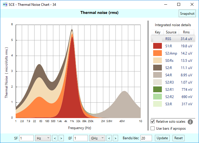
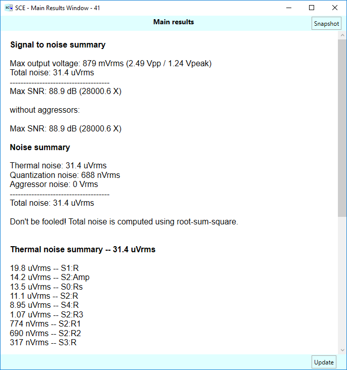
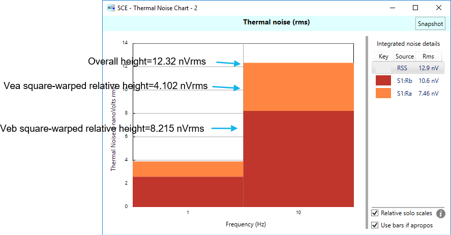
The right side of the thermal chart gives a legend showing each noise source (in our case, the two resistors), along with the overall noise contribution of that choice.

Overall noise results

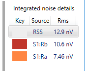
For example, the label “S1:Rb” stands for “resistor Rb of Stage #1, and we show an overall noise value for that resistor as 10.6 nVrms. The label “S1:Ra” stands for “resistor Ra of Stage #1”, and we shown an overall noise for that resistor as 7.46 nVrms. At the top of the legend we show the overall noise of the system, labeled as “RSS” (which stands for Root-Sum-Square) given as 12.9 nVrms. So how do these numbers correlate to what we just calculated? Next, we’ll take a look at how that’s done. And by the way, you are probably wondering about the different colors in the chart — and the heights of the bars. These will be explained in due course.

Let’s see how the overall noise (that is, over all the frequencies of interest) for Rb is computed. The way thermal noise works, being Gaussian and all, is that if you want to compute total noise, you take each individual rms value, square it, add the squares together, and then take the square root of the result. This is called the root-sum-square method. So the formula for Rb’s overall contribution of noise is

\(\displaystyle Ve{{b}_{{overall}}}=\sqrt{{Ve{{b}_{{band1}}}^{2}+Ve{{b}_{{band2}}}^{2}}}=\sqrt{{{{{3.182}}^{2}}+{{{10.06}}^{2}}}}=10.55\ {{nV}_{{rms}}}\)

We’ve rounded this to 10.6 nV in the chart legend.

Likewise, for Ra, we have:

\(\displaystyle Ve{{a}_{{overall}}}=\sqrt{{Ve{{a}_{{band1}}}^{2}+Ve{{a}_{{band2}}}^{2}}}=\sqrt{{{{{2.248}}^{2}}+{{{7.109}}^{2}}}}=7.4556\ {{nV}_{{rms}}}\)

which we’ve rounded to 7.46 nV in the chart legend.

Okay, what about total noise in the system? Well, we do the same root-sum-square trick — just at a higher level. We square each noise source’s contribution, add the squares together, and take the square root of the result:

\(\displaystyle Tnois{{e}_{{overall}}}=\sqrt{{Ve{{a}_{{overall}}}^{2}+Ve{{b}_{{overall}}}^{2}}}=\sqrt{{{{{7.4556}}^{2}}+{{{10.55}}^{2}}}}=12.92\ {{nV}_{{rms}}}\)

which we’ve rounded to 12.9 nV in the chart legend.

There’s a lot of root-sum-squaring going on when thermal noise calculations are involved. Thankfully, SCE does all this tedious work for us.

Next, we take a look at the bars in the chart itself, and show how to interpret the heights and colors of the bars. Let’s look at the first band to get things started:

relative noise band one II

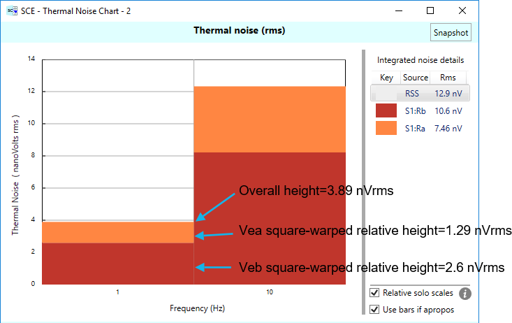
The first thing to note is that each band is composed of different colored rectangular bars stacked vertically. The bar colors correspond to those given in the chart legend. In this case, the red color is for Veb, the thermal noise due to resistor Rb. The orange color is for Vea, the thermal noise due to Ra. The noise contributions of the various sources are sorted such the that source with the most overall contribution (over all the bands) is drawn first, on the bottom. The source with the second most overall contribution has it’s contribution rectangle stacked on top of the first, and so on. The relative heights of these rectangles are such that, when added together, they represent the overall thermal noise for that given band. Next, we explain in detail how these heights are computed.

First, the overall noise contribution for the first band: In our example, we have the two values we calculated earlier:

\(\displaystyle Ve{{a}_{{rto\ first\ band}}}=1.3333\ nV/\sqrt{{Hz}}\times \sqrt{{2.844\ Hz}}=2.248\ {{nV}_{{rms}}}\)

\(\displaystyle Ve{{b}_{{rto\ first\ band}}}=1.8867\ nV/\sqrt{{Hz}}\times \sqrt{{2.844\ Hz}}=3.182\ {{nV}_{{rms}}}\)

If you add these up using root-sum-square, (remember, these are Gaussian values represented in RMS form) you end up with the overall noise contribution for the logarithmic band centered at 1 Hz:

\(\displaystyle {{V}_{{noise\ first\,band}}}=\sqrt{{{{{2.248}}^{2}}+{{{3.182}}^{2}}}}=3.896\ {{nV}_{{rms}}}\)

What about the relative heights of the colored bars? We’d like to graphically display how much each source contributes to the overall noise, relative to the others. There are many different mappings that could be used — a linear mapping, for example. But note how the noise contributions are squared before summing. Due to this squaring, the higher the noise source’s contribution, the more it will tend to dominate the overall result. The relative proportion is, for sure, not linear. SCE accounts for this by using a “square-warping” when determining relative heights:

\(\displaystyle RelativeNois{{e}_{i}}=(Nois{{e}_{i}}^{2}/Overal{{l}_{{noise}}}^{2})\times Overal{{l}_{{noise}}}\)

Take noise source Ra, for example. It’s relative noise contribution for the first band can be computed (using the overall noise for the first band that we computed earlier) as:

\(\displaystyle RelativeNois{{e}_{{Ra\ first\ band}}}=({{2.248}^{2}}/{{3.896}^{2}})\times 3.896=1.297\,n{{V}_{{rms}}}\)

Likewise for Rb:

\(\displaystyle RelativeNois{{e}_{{Rb\ first\ band}}}=({{3.182}^{2}}/{{3.896}^{2}})\times 3.896=2.6\,n{{V}_{{rms}}}\)

If you add these relative heights together, you’ll get back to overall noise contribution for the first band. (Well, there is some round-off error due to how we’ve presented the calculations here:)

\(\displaystyle {{V}_{{noise\ first\ band}}}=1.297+2.6=3.897\ n{{V}_{{rms}}}\)

To recap: We’ve arranged the relative heights of the noise contributions so that they reflect the square-domination of the bigger noise sources, but in such a way that when the stacked heights are added together, the result accurately reflects the overall noise for the given band.

Let’s now do the same for the second band.  Here’s the graph annotated:

relative noise band two

First the individual source contributions:

\(\displaystyle Ve{{a}_{{rto\ second\ band}}}=1.3333\ nV/\sqrt{{Hz}}\times \sqrt{{28.44\ Hz}}=7.109\ {{nV}_{{rms}}}\)

\(\displaystyle Ve{{b}_{{rto\ second\ band}}}=1.8867\ nV/\sqrt{{Hz}}\times \sqrt{{28.44\ Hz}}=10.06\ {{nV}_{{rms}}}\)

Computing the overall contribution for band 2:

\(\displaystyle {{V}_{{noise\ second\,band}}}=\sqrt{{{{{7.109}}^{2}}+{{{10.06}}^{2}}}}=12.32\ n{{V}_{{rms}}}\)

Next, the relative contributions:

\(\displaystyle \begin{array}{l}RelativeNois{{e}_{{Ra\ second\ band}}}=({{7.109}^{2}}/{{12.32}^{2}})\times 12.32=4.102\,n{{V}_{{rms}}}\\RelativeNois{{e}_{{Rb\ second\ band}}}=({{10.06}^{2}}/{{12.32}^{2}})\times 12.32=8.215\,n{{V}_{{rms}}}\end{array}\)

These add up to the original band 2 overall noise:

\(\displaystyle {{V}_{{noise\ second\ band}}}=4.102+8.215=12.32\ n{{V}_{{rms}}}\)

To double check our results, let’s root-sum-square (RSS) the heights of the two bands, and see if we get back the overall noise in the system of 12.92 nVrms:

\(\displaystyle \sqrt{{{{{3.986}}^{{2+}}}{{{12.32}}^{2}}}}=12.92\ n{{V}_{{rms}}}\)

Before, we calculated the overall noise by RSS’ing the individual noise source contributions. Here, we’ve calculated the overall noise by RSS’ing each band’s contributions. The end result is the same.

We’ve had a colleague say to us that SCE is “just a giant spreadsheet.” Well, that’s true in a sense. And the above calculations show how the thermal noise calculations have a spreadsheet/matrix-like feel to them. Just be glad you don’t have to implement this spreadsheet yourself — especially as your circuits get more complex than a simple voltage divider. The computations for thermal noise referred to output in arbitrary circuit configurations get rather complicated in a hurry. Be glad that SCE is on your side, doing these calculations for you, automatically.

Okay, so far we’ve used a very coarse resolution for our thermal noise charts. Next, we’re going to increase that resolution and see how that affects the look and feel of the charts. First, we’ll go from 1 band per decade to … two bands per decade. Yes, we’re feeling rather adventurous! Here’s the resulting chart:

chart with 2 bands per decade

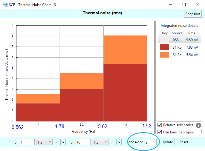
We denoted the start and end frequencies of each band using blue labels, and as before, these labels don’t actually appear on the real chart. We just show them here to help in understanding how the bands work. The main upshot is to notice that the bands are smaller in frequency width than before, and that this means the “spill over” at the ends of the 1 – 10 Hz frequency range is smaller. These two facts mean that: (a) The heights of each band are going to be shorter, since there is less bandwidth to cover, and (b) the overall noise is going to be less than we got before — in this case, 9.59 nVrms, instead of 12.92 nVrms. Note that the chart above, with more resolution, is the more accurate one. And as you might expect, if you increase the resolution (bands per decade) even further, you’ll get even more accurate results.

So far, we’ve drawn the charts using rectangular bars. That’s because we’ve checked the box that says “Use bars if apropos” at the bottom of the legend. (This box is checked by default.) With this box checked, SCE will plot using rectangular bars as long as the number of rectangles produced isn’t too large. Once a certain threshold is reached, SCE reverts to drawing polygon curves. Next, we’ll see that in action, but we’ll force the polygon curves by turning off the “Use bars if apropos” checkbox, leaving all other parameters alone. We end up with the following chart:

annotated two band chart using polygon curves II

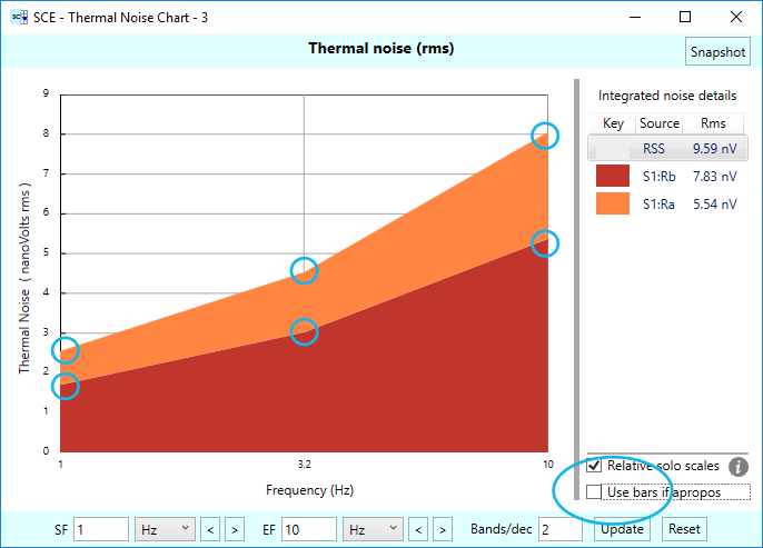
We’ve annotated this chart with blue circles and ovals to indicate key features of the changes made. As before, these annotations don’t appear on the real chart.

Instead of drawing rectangular bars with the bar centers aligned with the center point frequencies of our bands, instead, we draw polygon curves, with the Y-value of each point of the polygons corresponding to the height for a given band, and the X-axis location is at a corresponding center point frequency. Also, notice the subtle shift in the X-axis labels, to accommodate this shift in how the points are drawn. (Compare with the previous “bar chart”.) The graph starts and ends at 1 Hz and 10 Hz, instead of before and after these frequencies.

Alrighty then, let’s get even more adventurous and move on out to … 20 bands per decade! Woohoo! Here is the resulting chart:

2016-08-25 (4)

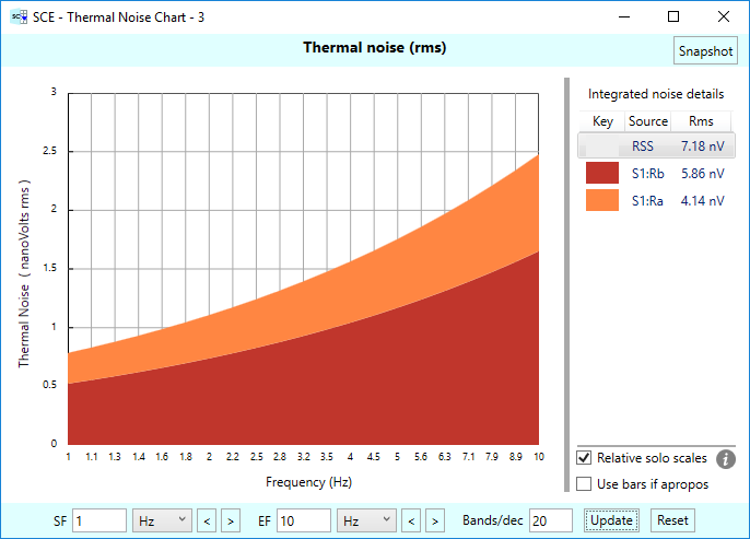
Note how our polygon curves are getting smoother. But do note: The results can be misleading, since the only data points that are known for sure are at the center point frequencies. In-between those frequencies? We don’t really know. There might be a spike, for instance, that gets completely missed. So sometimes it behooves you to experiment with higher resolution to see if you’ve missed anything.

With the smaller bandwidths, the resulting overall noise calculations are getting more accurate. Now how the chart is saying 7.18 nVrms total noise, instead of the 12.92 nVrms we originally got for one band per decade, and the 9.59 nVrms we got for two bands per decade.

It’s been our experience that, in general, 20 bands per decade gives you reasonably accurate results — unless your circuit’s response has resonances that can spike. In cases like that, you might want to try 100 bands per decade, or even higher, to try and capture those spikes.

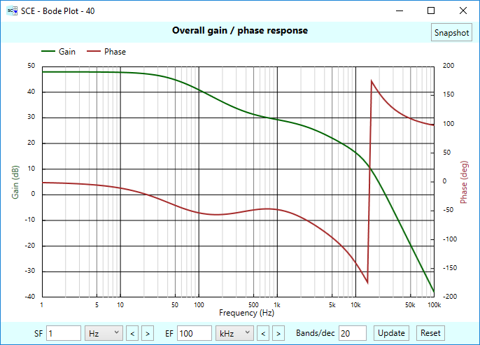
So far, we’ve kept our frequency range covering 1 to 10 Hz. The overall noise computed in the chart is based solely on that frequency range, but as we mentioned earlier, thermal noise is white, and as such, covers all frequencies. What happens if we cover more in our chart? Let’s see what happens if we extend our frequency range out to 100 Hz. To do this, the easy way is to use the frequency range extension buttons on the right side, which manipulate the ending frequency. (There are corresponding buttons for the starting frequency on the right side). Each click on the outward right-arrow button extends the frequency by a decade, as shown below:

chart out to 100 Hz

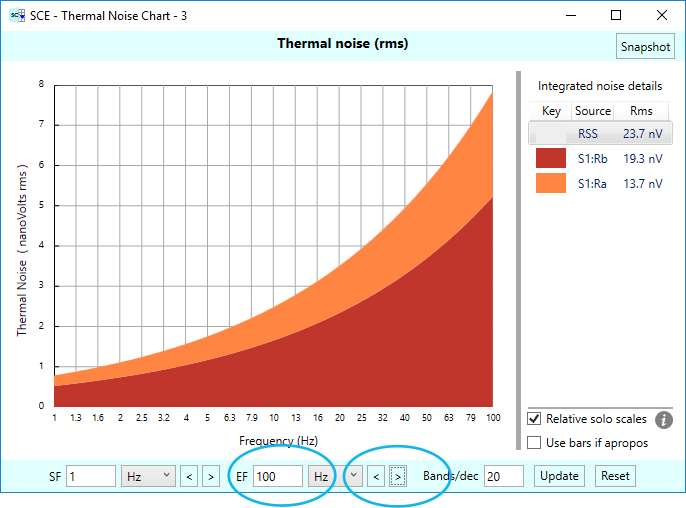
Notice how the noise is rising at the higher frequencies. Our total noise is up too, from 7.18 nVrms to 23.7 nVrms. What gives? Two things: (1) Remember, thermal noise is white, covering all frequencies, (2) At the higher frequencies, the bandwidth of each band is wider too — in a logarithmic fashion. A wider bandwidth means more noise in that band. The end effect is the noise appears to be rising exponentially in the chart. It isn’t really, it’s just that appears that way as the bands get wider and wider. What’s really happening is that the white noise, if plotted on a linear chart, would be a straight line. But since our thermal charts are logarithmic in nature, those straight lines get morphed into exponentially rising curves by the increasingly wider bands.

We’ve thought long and hard about this rising noise phenomenon, and whether the charts should be shown linearly instead of logarithmically — the root cause. There is no easy answer, but we deem the current logarithmic method better than all the alternatives, and besides, we reason that having the noise appear to be rising is a good thing — it may make the user panic just enough to realize that noise is occurring at high frequencies, and that it needs to be addressed. You should duly note that if you have an A/D converter in your signal chain, it samples that noise, regardless of frequency. This unfiltered high frequency noise can be a real problem. It can get intermodulated down into frequency ranges you’d rather it not.

Continuing on with extending the frequency range, we dip our toes deeper into the water and go out to 10 KHz by clicking the right side frequency range extender button a few times:

chart out to 10 kHz

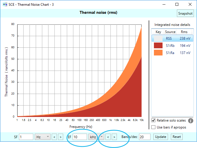
Now our total thermal noise is up to 238 nVrms. For our simple voltage divider circuit, which can’t filter out any high frequency thermal noise, this rising trend will continue — out to the THz range anyway. When the THz range is encountered, quantum effects kick in, as noted by Nyquist, and the thermal noise will start dropping off, all on its own. We’ll leave the demonstration of this effect for another blog post.

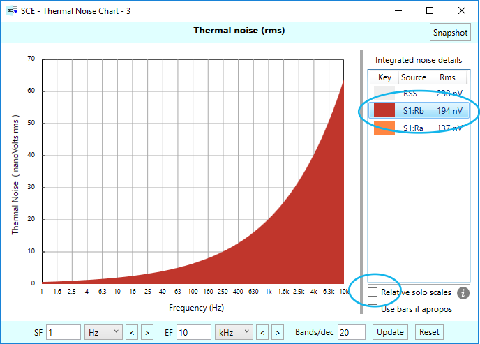
Next, we want to illustrate some of the other features of the thermal charts in SCE. In particular, we can isolate the thermal noise for a single noise source, and see it on it’s own. We do this by clicking on the appropriate noise source entry in the chart legend. For example, here is the result for S1:Rb:

Rb relative noise

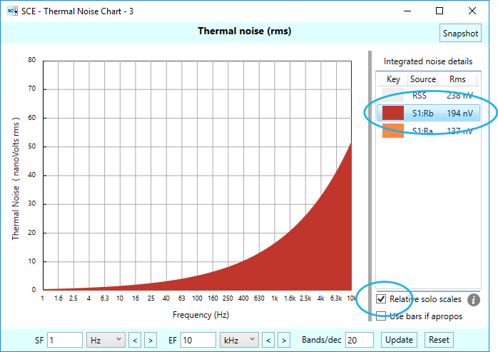
Soloing a noise source this way produces a plot with a single curve — in this case for noise from resistor Rb. The scale of the plot is “relative” — relative to the overall noise. This is accomplished by checking the “Relative solo scales” check box (which defaults to checked.) Notice the scale of the chart is the same as it was with the two noise sources combined, shown in the previous chart.

NOTE: If you want to go back to displaying all the noise sources, click the “RSS” label at the top of the legend.

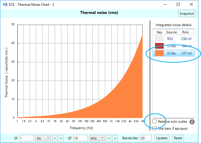
Let’s see what happens when we solo the Ra noise:

Ra relative noise

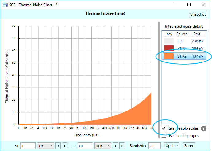
In case you are wondering about the max height of the noise in the chart (roughly 25 nVrms, occurring at 10 kHz) and how that corresponds to the value in the legend (137 nVrms): Remember, the legend is showing total RMS noise over all frequency bands for the noise source of interest. It’s in effect the integration of the area under the noise curve. (And the more bands per decade, the more accurate that integration.) But note this integration is accomplished via the root-sum-square of each band’s contribution.

Sometimes the relative size of the noise sources is dramatically different, and some noise sources may be small enough to not show up at all in the relative plots. In that case, you can uncheck the “Relative solo scales” check box, so that the noise is plotted to its own natural scale. Our voltage divider example doesn’t have this problem, but we’ll show you have to handle such cases anyway: You turn off the “Relative solo scales” checkbox. Here are our two noise sources plotted with the relative scale turned off. Notice how the Y-axis scale of the charts changes to accommodate the natural ranges of the two noises:

RB noise auto-scaled

Ra noise auto scaled

In this voltage divider example, the two solo thermal noise plots have the same shape — these are simple resistors after all. The only difference is in scale — that scale being determined by the referred-to-output voltage divider ratio.

Okay, we’ve covered most of the details of the thermal noise chart. We haven’t covered the Update and Reset buttons — or have we given a detailed description of how to use the frequency ranges at the bottom of the charts. We’ll cover these features in a subsequent blog post. But for now, we’d like to show a more interesting thermal noise chart, using a more complicated circuit.

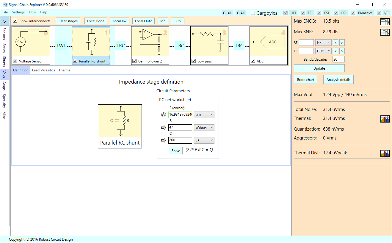
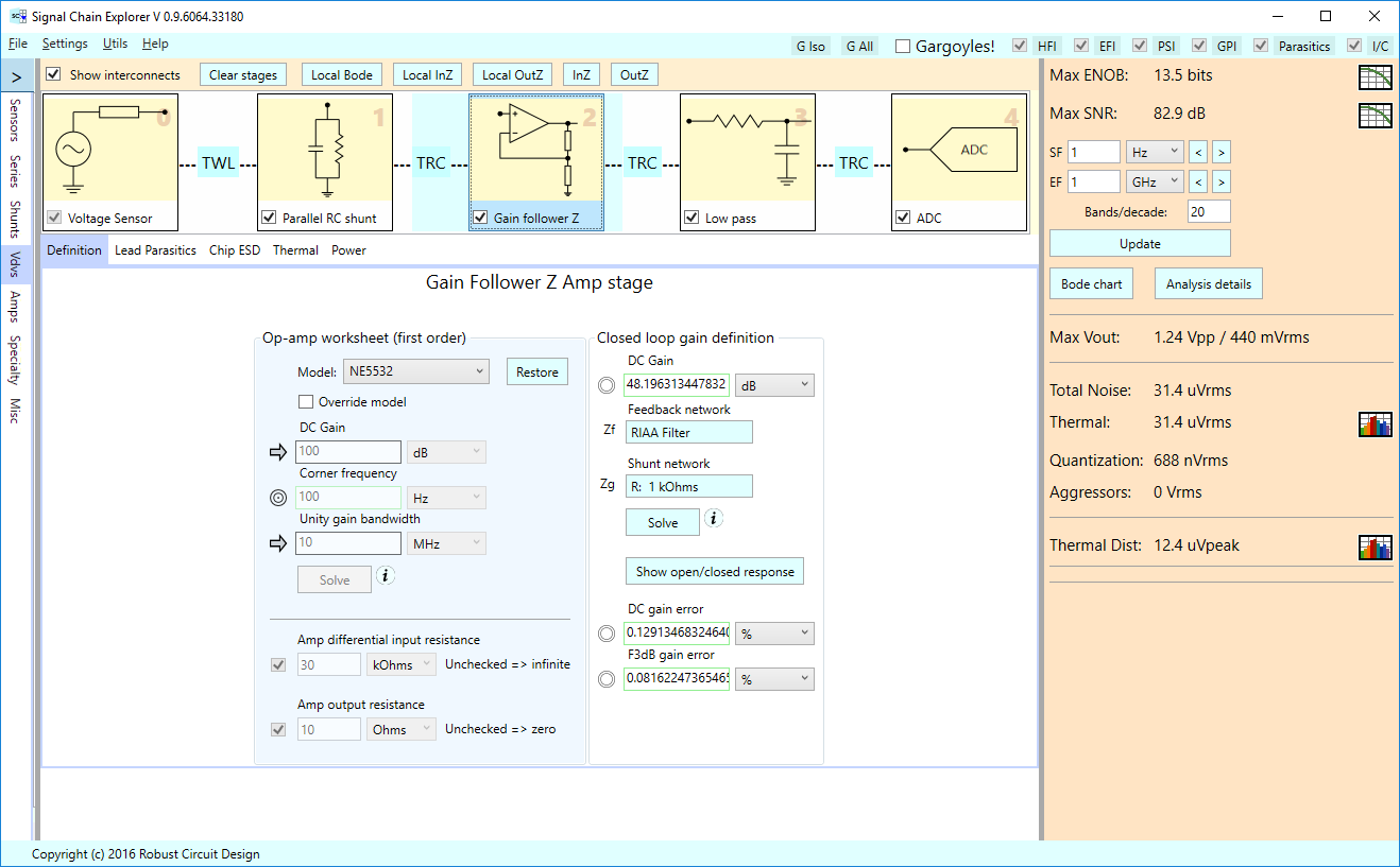
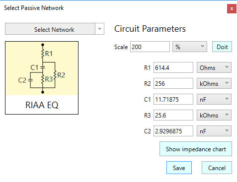
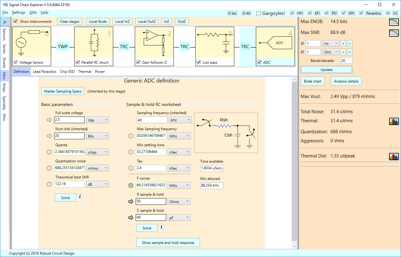
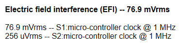
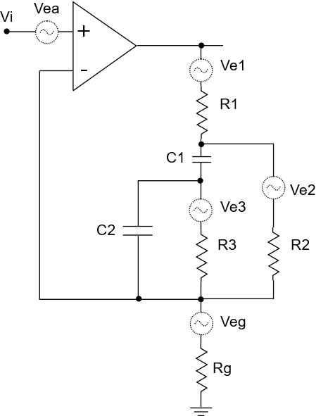
In this more complex example, we have a non-inverting “gain follower” amplifier stage, with a RIAA equalization filter in the feedback path. This stage has multiple noise sources: the feedback path resistors, (there are three of them), a resistor shunting to ground, and another noise source we haven’t talked about: the amplifier itself.

Op-amps have resistances: In the transistor gateways, the compensation networks, current sources, and what have you. The actual configuration is of course, implementation dependent. These resistances, like all resistances, contribute thermal noise, and fortunately for us, op-amp manufacturers usually include a noise specification in their op-amp datasheet that covers all these noises and sums them up into a single number. For example, an NE5532 op-amp has around 5 nV/rootHz of thermal noise, according to the datasheet for this part.

We model the thermal noise of an op-amp by injecting an error voltage at one of the input pins. For our non-inverting stage, we inject it at the positive pin. Here is the closed-loop amplifier stage in all its glory, with noise error voltages added for the amplifier and all the external resistors in the circuit:

RIAA Amplifier

Here is the thermal noise chart for this circuit, using a NE5532 op-amp, and plotted from 1 Hz to 100 kHz, 20 bands per decade:

2016-08-25 (11)

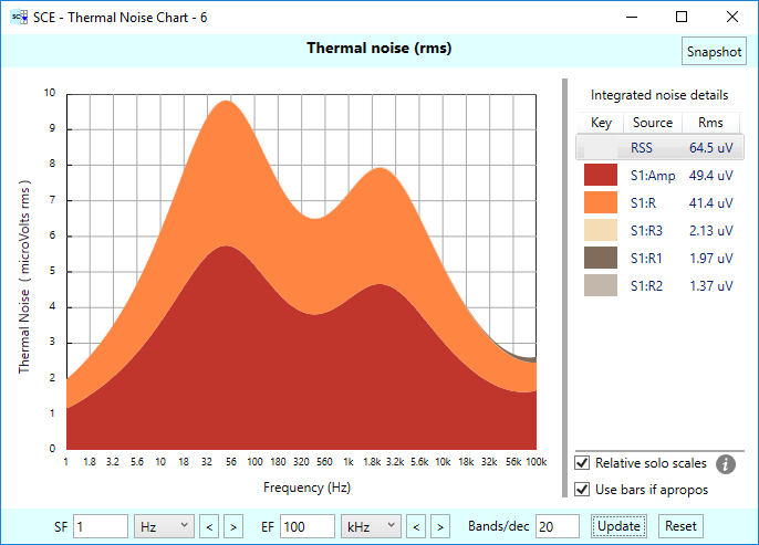
From this chart, we see that the amplifier itself contributes the most noise, followed closely behind by the resistor to ground (denoted as S1:R in the chart). The feedback resistors contribute much smaller amounts. One is barely visible in the stacked chart, the other two aren’t visible at all. You can experiment by soloing these noise sources to see their relative shapes, but since some of them have such small areas relative to the others, they won’t really show up. Fortunately, you can turn off the “Relative solo scales” checkbox, and see them self-scaled. We show all the noise sources plotted this way in the following figure. Do note that each plot has a different Y-Axis scale. Don’t be fooled!

self scaled solo plots II

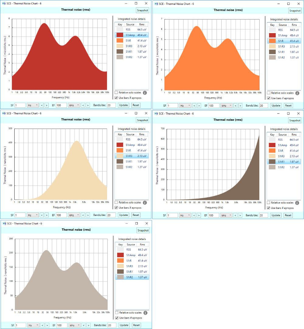
NOTE: If you experiment by clicking the “Relative solo scales” checkbox on and off for a soloed noise source, you might see the resulting plot not only change scale (and/or size), but it might change shape as well. What gives? Remember that with relative scaling, the noise for a single source is plotted relative to the other noise sources, using a square-warped mapping. Turning off relative scales gets rid of this warping. Also, a noise source’s “height” in the relative scales depends on what the other noise sources are doing, so if a noise source is large for a particular frequency band, but the other sources are not, that first noise source will take on a much larger height than it would otherwise, if plotted on its own without relative scaling.

As before, we are only showing a portion of the frequency range. You can experiment and see what happens out at higher frequencies. You might be surprised! (And we note that we’ll be covering the really high frequencies — such as a THz, in a subsequent blog post.)

Conclusion

You’ve now had a solid introduction on how to interpret the thermal noise charts in SCE. When I told a colleague how long this post was turning out to be, he asked, “How can such a post be that complicated, with just a simple voltage divider?” Well, it’s because even though SCE computes and plots thermal noise almost instantaneously with little effort on your part, there’s a lot going on under the hood. Just be thankful you don’t have to do this by hand!

One final thing to point out: In the last example involving an amplifier stage, we plotted all the solo noise contributions, and you got to instantaneously see their shapes, however small. That’s a lot of power at your fingertips, and we wonder if this type of clearly visualized behavior has really been seen before, with such ease.

If you’re lucky, thermal noise is often small, so small it may be hard to see in a real circuit with a scope. It’s in that class of sometimes-invisible phenomenon that we hope to make visible in SCE. Who knows, for example, what someone might uncover looking at the tiny shapes of the thermal noise in each of the resistors in an RIAA feedback network. Maybe you’ll be the one to uncover some great secret!

Bon voyage on your explorations! And good luck.


Posted in SCE Manual, Signal Chain Explorer | Tagged Johnson-Nyquist noise, thermal noise, thermal noise charts | Leave a reply

Simple Digitized Audio Example

Robust Circuit Design Posted on August 19, 2016 by adminOctober 28, 2016

In this Short and Sweet blog post we’ll take a quick look at using Signal Chain Explorer to analyze a simple vinyl-to-digital audio signal chain, consisting of a Shure M97XE vinyl cartridge pickup, a twisted pair connection to a parallel RC termination shunt, then an amplifier stage including RIAA equalization, a low pass filter, and finally an A/D stage.  The idea here is to show you the kind of construction and analysis that’s possible with SCE.

Overall Signal Chain and Results

The figure below shows the overall signal chain, along with the analysis results of an SNR of roughly 89 dB, (14.5 effective number of bits.)

2016-08-19 (10)

The upper right portion of the main window is the main focus of SCE, showing you the signal to noise ratio and effective number of bits, in this case, 88.9 dB and 14.5 bits. As it turns out, it’s difficult to digitize vinyl audio to even 16 bits of resolution, and you have to jump through a lot of hoops to get that.

The signal chain shown here is not meant to represent the ultimate in phono audio digitization — far from it — but rather, to show you the basics of constructing a signal chain in SCE that processes a phono audio signal and prepares it for digitization. Next, we’ll walk through each of the stages.

Shure M97XE Cartridge Sensor

We start with a “sensor stage”, which in this case represents a Shure M97XE cartridge, having 1550 ohms of series resistance, and 650 mH of series inductance per the Shure data sheet. We’re using a nominal output voltage of 5 mVpeak, which is a rough representative of what the device can deliver. (It’s spec’ed at 4 mVpeak at 1 KHz, using a 5 cm/sec recording velocity.)

SCE not only models the stages, it also models the interconnects between the stages, be they wires or traces. Here we’ve connected the sensor stage to a shunt termination stage via a twisted pair interconnect, as shown in the next two screen shots: (1) A summary of the interconnect model, and (2) the geometry used, in particular, an arbitrary 600 mm length. For the other stages, we’re using “trace” connections, that is, 14mm long PCB traces.

2016-08-19 (11)

2016-08-19 (12)

Cartridge Termination Stage

We terminate the sensor connection with a parallel RC shunt, using a 47 kOHm resistance and 200 pF capacitance, as recommended by the Shure data sheet:

2016-08-19 (2)

NE5532 Amplifier Stage with RIAA Equalization

Next, we follow with a single non-inverting amplifier stage (which is called a “voltage gain follower” or “gain follower” in SCE terminology). This gain follower stage is deemed “generic” because we can insert any passive network into the feedback loop, as well as the shunt to ground: In this case, we’ve inserted an RIAA filter into the feedback loop, and a simple 1 kOhm resistor to ground. The closed loop gain definition worksheet on the right side of the stage definition panel below shows this configuration, and we follow that with a screen shot of what the RIAA filter looks like:

2016-08-19 (3)

2016-08-19 (4)

In this amplifier stage, we’ve chosen an NE5532 op-amp which has a DC gain of roughly 100 dB, and a unity gain bandwidth of roughly 10 MHz, as shown in the op-amp worksheet on the right side of the stage definition panel given two screenshots earlier.

One of the useful features of SCE is the ability to compare the open-loop and closed-loop response of an amplifier stage, as shown below for our NE5532 stage with RIAA equalization:

2016-08-19 (13)

From the closed-loop response you’ll notice a pole at 50 Hz, a zero at 500 Hz, and a pole at 2 kHz. These roughly represent the appropriate RIAA equalization response.

Low Pass Filter Stage

Before the A/D converter, you almost always want to place a low pass filter to reduce any high frequency noise being digitized. Here, we’ve chosen a simple RC filter with a 40 kHz corner:

2016-08-19 (5)

Along with the open-loop, closed-loop plots shown earlier, another useful feature of SCE is the ability to see the “local” Bode plot of any stage. By “local,” we mean the stage in isolation. Here’s the local Bode plot of our RC filter, clearly showing the 40 kHz corner:

2016-08-19 (14)

Generic A/D Stage

Next, we’ve incorporated a “generic” A/D stage. (By “generic”, we mean we aren’t specifying the A/D to great detail, but instead, only looking at it as a sample & hold device with a given full scale range and bit resolution.) We’ve chosen a 20 bit device (we choose that many bits to keep the quantization noise down) having a 2.5 Vpp scale, and are sampling at 40 kHz (arbitrarily chosen.)

2016-08-19 (17)

Overall Bode Plot

That’s the whole signal chain. What kind of analysis can we do? First, here’s the overall Bode plot:

2016-08-19 (18)

Before you get too scared seeing how much the response drops off at higher frequencies (the 20 kHz response is down roughly 40 dB from the 10 Hz response), remember that the purpose of the built-in RIAA equalization is to reduce the artificial boosting of the high frequencies induced at recording time.

Thermal Noise Sand Paintings

One of the main features of SCE is the ability to see how much thermal noise is injected into our signal chain. Here’s the thermal noise vs frequency plot for our overall system, shown in a form we like to call “thermal noise sand paintings:”

2016-08-19 (7)

The thermal noise chart is vertically “stacked”. At each frequency, the contributions of each noise source are stacked together, using a RMS-warped scale. The overall height of the curve represents the total RMS noise at a given frequency, and if the whole curve is integrated as a whole, you get the overall RMS noise of the system. In our case here, the noise from the 47 kOhm termination resistor (shown in red) dominates the noise, particularly in the 11 kHz region. Also, notice thermal noise rearing its ugly head out at 50 MHz. This is noise from the sample and hold resistance in the A/D that cannot be filtered out. And do note, the A/D will sample this noise, no matter the frequency, and that this noise can intermodulate down into the audible range. Your only alternative is to use a smaller resistance (and thus higher capacitance) in the sample and hold, or to cross your fingers that the intermodulated noise isn’t too audible.

The overall thermal noise of our system is 31.4 uVrms, compared to a signal of roughly 2.5 Vpp (or 879 mVrms). There is also noise due to quantization in the A/D, though in this case it’s down in the nV region. We can inspect the noise contributions in detail using the “Analysis Details” button. Here is the Analysis Details dialog:

2016-08-19 (19)

Thermal Transient Distortion Plots

Another unique feature of SCE is the ability to calculate thermal transients (error voltages) caused by the transient change in resistance of components due to heating — in this case, the resistors and any op-amps in the circuit. SCE uses fairly simple worst-case models that give you ballpark estimates of the worst you can expect (that is, it assumes each part’s thermal environment is decoupled from others and/or that the induced errors just happen to swing whatever way gives the worst results.) Here’s the thermal transient plot for our system:

2016-08-19 (8)

Gargoyles

Last but not least, the most unique feature of SCE is its “gargoyles.” Gargoyles are circuit parasitics plus external aggressors. So we model things like lead parasitics, interconnect parasitics, and then aggressors such as magnetic interference and electric field interference. We also get a handle on power supply ripple interference, and ground plane interference as well. The models used in the current versions of SCE are admittedly simplistic, but they give you a sense of the scale of these problems. It’s invaluable to be reminded that these interferences, these gargoyles, can really make a mess of your signal chain.

For example, the two screenshots below show the detailed results of turning on the default gargoyles. These defaults include a microprocessor clock line placed too close to the signal line, improperly filtered 60 and 120 Hz ripple from a switching power supply, and interference coupling into our twisted pair leads going from sensor the shunt termination, as well as into the traces between the other stages. Also included are voltage errors induced by non-zero ground plane resistance. Notice how our nice 89 dB SNR (14.5 bits ENOB) gets cut almost in half to 49 dB (7.85 bits).

First, the SNR summary and the thermal noise summary with gargoyles turned on:

2016-08-19 (20)

Second, the details of the aggressors. Here EFI is electric field interference, HFI is magnetic field interference. GPI is ground plane interference. And PSI is power supply interference:

2016-08-19 (21)

Wet your appetite?

This has been a whirl-wind tour through the modeling of an phono audio analog to digital signal chain, including all the things that can interfere with the signal. We didn’t expect you to understand everything that’s going on in the dialog boxes at first glance, but we wanted to give you a flavor of what’s possible with SCE. We hoped we’ve wetted your appetite!

Posted in Short and Sweet, Signal Chain Explorer | Tagged Bode plots, EFI, GPI, HFI, NE5532, PSI, Shure M97XE, thermal distortion, thermal noise | Leave a reply

LC Baluns In Action

Robust Circuit Design Posted on August 1, 2016 by adminNovember 28, 2016

A new feature of Signal Chain Explorer (SCE) is the ability to use LC balun circuits. In this Short and Sweet article we’ll show how SCE can be put to use in inspecting the behavior of these strange but useful creatures.

What Be These Baluns?

The word “balun” stands for “balanced-to-unbalanced.” It’s a circuit that takes a balanced, differential signal and turns it into a single-ended (grounded) circuit. Baluns also work the other way, from single-ended to differential. It’s the latter that we’re going to show. In our discussion, you’ll see some of the new features of SCE that make analyzing such circuitry easy and intuitive.

Along with converting differential to single and vice versa, a balun can also perform one other important task — impedance matching. An example is shown below, where we wish to take a single-ended 50 Ohm source and match it to a 300 Ohm balanced load. The balun does the work to perform this transformation:

High Level Circuit II

In general, baluns come in both wide band and narrow band configurations. Wide band baluns are usually implemented with coils wrapped around some type of ferrite material. They are cousins to the transformer family. Narrow band baluns can be implemented using a circuit consisting of only lumped Ls and Cs. These are called LC Baluns. We show the details of such a circuit below:

LC Balun single to differential

LC Balun single to differential


An LC Balun single-to-differential circuit works by taking a single-ended signal and passing it through two pathways: a second order low-pass filter made from an L and C, and a second order high pass filter, also made from an L and C. (Shown is an optional DC-blocking capacitor, Cg, on the second filter, which can be used for ground isolation. We won’t be using that here. Pretend it’s not there.)

Having no resistive elements, these filters have sharp resonant frequencies. In fact, since they have the same L and C values, they have the same resonant frequency, which can be determined by the following formula:

\(\displaystyle {{f}_{0}}=1/(2\pi \sqrt{{LC}})\)

Because of this resonance, LC baluns are narrow band. They can be used when you have a single frequency you wish to process. They are not appropriate if your signal covers a wide band.

Two filters working in concert

It’s instructive to see what the top and bottom filters of the LC Balun do. Here is a Bode chart (produced by SCE, the production of which is outside the scope of this paper) of the top filter, showing the transfer function from the input voltage Vi, to the output voltage Va:

Low pass LC response

This filter starts out with 0 dB gain, and a phase of 0. At the resonant frequency the gain spikes (theoretically to infinity) and the phase does a rapid transition to -180 degrees. At the spike, the phase will be -90 degrees. After the spike, the gain tapers off, eventually at a -40 dB/decade rate.

Be aware that the spike really doesn’t go to infinity in the real world, due to parasitics in the components (for example, a bit of resistance in the capacitor and inductor.)

The bottom filter works in reverse: as a “high pass” filter, whose response is shown below in the Bode plot of the transfer function from the input voltage Vi to the output voltage Vb:

High pass LC response

This filter attenuates lower frequencies, the gain going upwards at a 40 dB/decade rate, until rising to spike once again at the resonant frequency. The phase is at a constant 180 degrees until resonance, and once again, we see a rapid transition in phase, this time, from 180 to 0 degrees. Right at resonance, the phase is +90 degrees. After resonance, the gain tapers off and settles to 0 dB. The phase, to 0 degrees.

In the time domain

You can see, then, that the two filters of an LC balun have -90 and +90 degree phase shifts at  resonance. Combined, they can form a proper differential signal (Va – Vb). To see this, here is a time-domain plot contrasting the input voltage Vi with the two output voltages Va and Vb. (Disclaimer: This plot was not created with SCE, since it currently only handles values in the frequency domain.)

LC Balun Plot 10

Besides the phase shift on the two output signals, you’ll notice a gain of 1.75 on each signal. We’ll talk about that gain in a bit.

Here’s a another plot contrasting Vi with the differential voltage Vdiff = Va – Vb. Notice we now have a differential gain of 3.5:

LC Balun Plot 11

Exploring LC Baluns in SCE

Let’s see how we can implement our balun circuit in SCE. The first thing to do is chop the circuit into a sequence of “stages”. There are three stages here: (1) The sensor stage, (20 the balun stage, and (3) the load stage. Here’s how the signal chain looks in SCE after adding these stages:

Signal Chain

You might wonder about the shunt stage, which we show going to ground. SCE was originally designed to handle only single-ended signals. It currently has no understanding of the differential variety. Since LC Baluns are a brand new addition, we haven’t had time to integrate the notion of differentiality. Not to worry, though. As far as understanding circuit behavior such as gain and impedance, we can pretend the differential signals are single-ended.

Let’s take a look at these stages in detail. The sensor stage incorporates a voltage source (arbitrarily set to 1 mVpp), with an optional series resistance and inductance. We’re using a resistance of 50 Ohms. That is, our sensor stage is the 50 Ohm source into the balun:

Sensor Stage

Next, the LC Balun stage:

LC Balun Stage

This stage incorporates one of the unique features of SCE: The use of equation worksheets. In this example, we have a worksheet that lets us pick a frequency of interest, the source resistance we’d like to convert, and the load resistance we’d like to convert into. From this, we can solve for the circuit components L and C by first pressing Solve to see the results, and then Apply to apply the component values for real to our balun.

The equations being implemented are as follows:

\(\displaystyle \begin{array}{l}X=\sqrt{{Rs\,RL}}\\\omega =2\pi {{f}_{c}}\\L=X/\omega \\C=1/(X\omega )\end{array}\)

In our example, we’ve designed the balun to work at 100 kHz, with a source resistance of 50 Ohms, and a load resistance of 300 Ohms. The latter is defined by a “shunt” stage (remember our discussion earlier about pretending we have a differential load):

Shunt Stage

With the stages defined and in place, we can click the Bode chart button in the main results panel to see the overall frequency response of this circuit. We’ve plotted it for a range of frequencies surrounding our target 100 kHz:

LC Balun Bode

This chart shows that our balun does indeed peak at 100 kHz, and has a gain — that we get “for free” from the LC resonance — of 1.75, the same gain we saw earlier in the first time domain chart for signals Va and Vb. Remember that SCE doesn’t yet understand differential signals, so it doesn’t know how to think in terms of differential gain. For example, our differential signal Vdiff in our earlier time domain chart shows a gain that’s twice what we see here.

Won’t you be my baluntine?

What about the impedance matching we promised earlier? Well, the idea with LC baluns is that they do their best matching at the resonant frequency, and we can see this quite easily with SCE, using the two buttons InZ and OutZ.

Input Impedance

The InZ button gives us an impedance plot showing the input impedance from the currently selected stage, all the way to the end of the chain. Here is a figure showing where the InZ button is located, and how to interpret its behavior:

Input impedance button II

WARNING: Don’t confuse the InZ button with the Local InZ button. The latter is an entirely different beast that we’ll talk about in later articles. But basically, the Local InZ button looks at the input impedance of the stage as though it were the only stage in the chain.

The result of pressing the non-local InZ button is given the impedance vs frequency plot shown below:

LC Balun InZ Annotated

This plot is a useful beast showing four types of data: The magnitude of the complex impedance in green, the real (resistive) portion of the impedance in blue, the imaginary (reactive) portion in red, and finally, the current that results from passing an arbitrary test voltage of 1V through the system, shown in turquoise. We are most interested in the impedance at the resonant frequency of 100 kHz. There, the reactance is zero, so we have a purely resistive impedance, and it’s right at 50 Ohms. Notice at the ends of the graph that the impedance is trucking on its way to 300 Ohms, in both directions. In fact, the impedance will be at this number at DC, and at infinite frequency.

What’s the significance of this chart? Well, our source impedance (from the sensor stage) is 50 Ohms. Our load impedance (in the shunt stage) is 300 Ohms. The balun stage serves to match these impedances by making itself look like 50 Ohms to the sensor stage, even though the balun stage has that 300 Ohm load hanging on it.

This only occurs right at the resonant frequency. Elsewhere, the matching isn’t so good, and gets progressively worse the further away from the center frequency we get. But that’s okay. We’re mainly interested in what goes on at 100 kHz. That’s the nature of using a narrow-band balun.

Output impedance

What about output impedance? The OutZ button gives us an impedance plot showing the output impedance from the currently selected stage, all the way to the beginning of the chain. Here is a figure showing where the OutZ button is located, and how to interpret its behavior:

OutZ Button Usage

Here’s the resulting plot:

LC Balun OutZ Annotated

From this plot, we see that the impedance becomes purely resistive at the resonant frequency, and that it’s right at 300 Ohms. That is, to the resistor load stage, the LC balun stage looks like a 300 Ohm source resistance, even though the stage itself has a 50 Ohm source. Once again, this is only true at our resonant frequency of 100 kHz. At the frequency extremes the balun stage looks like 50 Ohms.

Summary

In this Short and Sweet article, we’ve shown you how LC baluns work, and you’ve seen how Signal Chain Explorer can be used to help understand how they operate. In particular, the InZ and OutZ plots are quite handy. You can select a stage at any point in the signal chain and see what’s going on in terms of input and output impedance. That’s especially useful for things like impedance matching baluns, for you can easily verify that your baluns are doing what you desire.

Remember that LC baluns only work for narrow band signals. For wide band impedance matching, baluns made up of various kinds of transformer configurations are used. Do note that although SCE doesn’t currently have such types of baluns implemented, it does now have a basic transformer stage that you can try, which can be used for certain types of balun implementations. This new transformer stage, while basic, can model the parasitics that exist in real-world transformers —  parasitics that can trip you up. Be sure to have a look!

Posted in Short and Sweet, Signal Chain Explorer | Tagged LC Baluns, narrow band impedance matching | Leave a reply

New pre-release of Signal Chain Explorer V 0.965

Robust Circuit Design Posted on August 1, 2016 by adminAugust 1, 2016

We’ve been busy the past few months updating the Signal Chain Explorer program. Even though this is a “point-release”, a ton of new features have been added. Here are the highlights:

  • Numerous new filter stages:
    • Sallen Key low pass, high pass, band pass, and band reject filters
    • Multiple Feedback filters, in low pass, high pass, and band pass configurations.
    • New passive band pass and band stop LRC filters.
    • Some of the active filters are still a little rough around the edges, with new design worksheets to come.
  • LC Balun stages: Single to differential, differential to single.
  • Transformer stage: Models the core and winding parasitics as well.
  • Input and output impedance plots: Starting from any stage (and going to the beginning or end of the signal chain.)
  • Local input and output impedance plots: These pretend the stages are by themselves.
  • Local bode plots: Just the stages by themselves.
  • Built-in Op Amp database: We’ve added a small database that models op amps of varying ability. More will come later.
  • New improved interconnect GUI: We’ve brought the stage-to-stage interconnect modeling — a key feature of SCE, front and center in the GUI.
  • Smoother, faster thermal noise charts: Can also inspect individual noise sources.
  • Optimized calculation engine: We’ve optimized the underlying calculation engine to be much faster, and take far less memory. Can now handle hundreds of bands per decade with ease.

We’ll be adding new articles in the next few weeks that highlight the new capabilities of Signal Chain Explorer, starting with a new Short and Sweet article on LC Baluns, and how you can inspect them using the new Input and Output Impedance charts.

In the meantime, give the new program a spin by downloading a preview now!


Posted in Signal Chain Explorer | Leave a reply

Mitigating Clock Line Interference: Improving SNR by over 40 dB

Robust Circuit Design Posted on April 28, 2016 by adminOctober 28, 2016

Introduction

In this Short and Sweet article, we showcase the ability of Signal Chain Explorer (SCE) to model electric field interference (EFI) in a circuit. We use a simple signal chain composed of a sensor, amplifier, and A/D converter. To simulate EFI, we add a  5 V, 1 MHz microprocessor clock signal and place it 1 mm away from the signal line. With one click we can estimate the signal quality, as measured by the Effective Number of Bits (ENOB) and Signal to Noise Ratio (SNR). We’ll show two ways to help mitigate this interference: (1) By moving the clock line further away from the signal line, and (2) by adding a low pass filter. These simple steps can increase the SNR by over 40 dB.

Because of SCE’s built-in functionality, all of this can be accomplished by setting a few parameters, and using a few clicks here and there.

Initial Configuration

Here’s the initial circuit, which we can easily build with just a few clicks using the SCE stage library:

wp57 initial stages

Suppose our sensor outputs 1 mVpp, and has a 100 kOhm resistance. We can set these parameters in the Sensor Stage Definition Panel. We’re going to ignore any inductance in this simple example.

wp57 sensor stage

Using the Gain Follower Stage Definition Panel, we can set the amplifier stage to be non-inverting (that is, a “Gain follower”), having 60dB closed loop gain. We’ll use a 741-like op-amp. Here are the details:

Gain follower stage

To end the analog portion of our signal chain, we’ll use a 5 V, 12 bit A/D having 50 Ohms switch resistance, and 48 pF sampling cap, as set in the lower right corner of the Generic ADC Definition Panel:

ADC stage

Let’s first determine the signal quality before turning on any “gargoyles” (gargoyles = EMI + connection parasitics). Pressing the Update button in the upper right panel computes the signal quality for us, as shown below. Note the Gargoyles! Check Box is turned off for the moment. Though we have no interference, we do have thermal and quantization noise which degrade the signal. These properties are modeled automatically for us and are given in the lower part of results panel:

Initial results no gargoyles

We end up with roughly 7.5 bits, so even though we have a 12 bit A/D, some of that resolution is being wasted. Our corresponding SNR is just under 47 dB.

Thermal noise dominates the signal degradation, coming in at 1.58 mVrms, whereas quantization noise is 352 uVrms. These are in comparison to a 350 mVrms (roughly 1 Vpp) output signal.

Though our 1 mVpp input signal has been amplified to 1 Vpp, we specified a 5 Vpp A/D. So we aren’t using the full range of the A/D, and we could improve things somewhat by either choosing a different A/D with a 1 V full scale, or by given the signal more amplification. But we’ll leave things as they are, for the effects of not using the full range are not significant in this example.

Adding Clock Line Interference

The results we just gave are the ideal ones — there is no outside interference, and no trace connection parasitics. In particular, we don’t yet have the 5 V, 1 MHz clock line interfering with our signal chain. Let’s put that in play by placing the clock line just 1 mm away from our signal traces. Here are the settings in the Master EFI Dialog that do this for us:

Initial EFI Setting

Since this is a “master” setting, it applies to each interstage connection — in our case, between the sensor and the amplifier stages, and between the amplifier stage and the A/D converter. Each of these connections are modeled the same: The EFI is injected as an “error voltage”, in this case 5V as per our setting above. The effective capacitance Ce is computed using the assumed geometry of the interference — the clock line trace is placed in parallel to the signal line trace, using a parallel plate capacitance model. We’ll study this model in depth in later articles.

Interconnection model with EFI injection

Here’s an example of the worksheet used to compute the effective capacitance of the clock-line-to-signal-line geometry:

EFI Worksheet

In computing the values, a master set of parameters is used for lead parasitics and trace geometries, etc, but these can be modified individually for each stage. For simplicity, we leave them the same for all the interstage connections of our example.

To enable the clock line interference, we must turn on the Gargoyle flag, the EFI flag, and the Parasitics (for the interstage connections) flag. We leave the HFI (H-Field interference), PSI (power supply interference), and GPI (ground plane interference) check boxes off. These checkboxes are located at the top of the main screen. Pressing Update gives us the new results: We see a drop from 7.47 ENOB to 1.89 ENOB, the SNR also dropping from 46.7 dB to just 13.2 dB.

wp57 initial results with gargoyles

We’ve lost 33 dB of signal due to the pesky clock line. Inspecting the noise summary in the right side panel, we see that the aggressors (aka gargoyles) are now dominating the noise, contributing 76.9 mVrms of the 77 mVrms total. Popping up the Analysis Details Dialog, we can scroll down to the EFI section:

initial EFI analysis

The EFI shows up in two places: S1 (before Stage 1), and S2 (before Stage 2). These interstage connection points default to having the same geometry as mentioned earlier, but the first has the biggest effect, because its interference is subsequently amplified 1000x by the amp stage.

Mitigating the Effects of the Clock Line

How do we control this interference? There are two easy ways: (1) By moving the clock line further away from the signal line, and/or (2) using a low pass filter.

Let’s do the first, moving the clock line various distances away. The following table lists the results:

Distance ENOB SNR Noise
1 mm 1.89 bits 13.2 dB 76.9 mVrms
10 mm 5.16 bits 32.8 dB 7.84 mVrms
20 mm 6.07 bits 38.3 dB 3.92 mVrms
100 mm 7.31 bits 45.8 dB 786 uVrms
1000 mm 7.47 bits 46.7 dB 78.6 uVrms


These noise figures are in addition to the 1.58 mVrms of thermal noise and 352 uVrms of quantization noise. As we move the clock line further away, the thermal and quantization noise sources become predominant, so there is a point of diminishing returns in increasing the clock line distance. Not to mention, the latter distances, 100 mm and 1000 mm, are most likely impractical for most PCB  scenarios. So we’d probably choose distances on the order of 10 to 20 mm, and these will get us within a few bits of the best answer we can achieve, given the signal chain configuration so far (7.47 ENOB).

We’d like to do better than this 7.47 ENOB, so how do we go about it? We can use the second method mentioned earlier, by incorporating a low pass filter. Let’s place one in front of the amplifier stage, and give it a corner of 1 kHz.  (Thus we are assuming a signal slower than 1 kHz).

Results With Low Pass Filter

From the results panel, you can see we’ve improved the signal quality dramatically, from 1.89 to 9.25 ENOB, (13.2 to 57.5 dB SNR), an increase of 7.36 ENOB (44.3 dB). Remember, this is for the case when the clock line is 1 mm away.

By adding another stage, (the low pass filter), we’ve also added another stage interconnect, which by default is also susceptible to the global interference we’ve set — the 1 MHz clock line EFI. However, the capacitor in the low pass filter reduces this interference, both before and after the filter. The interconnect points are labeled as S1 and S2 in the following analysis details:

low pass filter EFI details

The EFI for these interconnects has been greatly reduced, down into nV territory. The S3 interconnect, between the amplifier and the A/D stages, hasn’t had its geometry changed, so it still has the same 256 uVrms noise it had before, but now it’s the dominant source of EFI.

We can experiment further by once again moving the clock line away, from 1 mm to 10 mm, for instance. If you do this and inspect the analysis details (not shown here) you’ll see that the clock line interference goes from 256 uVrms, to 25.6 uVrms, and we increase signal quality to 9.51 ENOB (59 dB). Note that as before, thermal and quantization still ultimately set the noise floor.

Conclusion

You’ve now seen the effects of a clock line placed too close to a signal line, in terms of EFI noise. We’ve shown how you can dramatically reduce these effects by moving the clock line further away. Sometimes you don’t have much room to maneuver in this regard, due to layout constraints, so a low pass filter might be used to further mitigate the noise.

For a 5V, 1 MHz clock line placed 1 mm away from our signal line, the following table shows how the initial signal quality drops, and then how you can gain that quality back by use of a low pass filter, and then move the clock line 10 mm away for even further gains:

Environment ENOB SNR
no clock line 7.47 bits 46.7 dB
clock line 1 mm away 1.89 bits 13.2 dB
clock line 1 mm away, low pass filter 9.25 bits 57.5 dB
clock line 10 mm away, low pass filter 9.51 bits 59 dB


To give a visual indication of signal quality, below are plots of a sine wave with various amounts of SNR. These randomized plots were produced using the sister product, Signal Wave Explorer:

Clean sine wave:

Clean sine wave

13.2 dB SNR sine wave:

13 db Sine wave

Sine wave with 59 dB SNR sine wave:

59 dB Sine Wave

We think you’d agree the latter signal is much preferable. We also think you can now agree that paying attention to electric-field interference in your circuit is important, and Signal Chain Explorer can help you quickly get a handle on the magnitude of that interference. You can easily explore the system-level tradeoffs in your circuit.


Posted in Short and Sweet, Signal Chain Explorer | Tagged clock line interference, EFI | Leave a reply

Capacitor Impedance

Robust Circuit Design Posted on February 22, 2016 by adminFebruary 22, 2016

In this Short and Sweet post, we take a brief look at how capacitors work and derive the formula for capacitor impedance, using Euler’s formula for complex exponentials. This post is a paraphrased excerpt from SWE Lesson 1.2.

A capacitor stores charge in the form of an electric field, or E-Field. In its most basic configuration it’s a pair of parallel plates, with an insulating material (or air, or vacuum) between them called the dielectric. When a voltage is applied across the plates, charges of opposite polarity accumulate on the plates, and an E-field develops.

Consider the following circuit, consisting of a battery, resistor, and capacitor, and a switch that allows the capacitor be charged and discharged.

Capacitor charging circuit

Suppose the capacitor is initially discharged (has no E-field), and then the switch is moved to connect the battery to the capacitor. Negative charges flow from the battery onto the lower plate of the capacitor, and these attract positive charges to the top plate. These positive charges can be thought of as negative charges (electrons) that have been displaced by leaving the top plate and returning to the battery. Thus a circuit is formed, and an E-field develops across the plate.

When a capacitor is charging (or discharging), there is charge flowing, and that means there is current. While you might think this means current flows through the capacitor, that is not the case, (at least not for an “ideal” capacitor). Charges move onto (or away) from the plates, but not across them. For this reason, the current associated with a capacitor is often called a displacement current.

A given capacitor can only hold so much charge, the amount being proportional to the voltage applied across the plates. The constant of proportionality is called the capacitance and the charge equation can be written as:

\(Q=CV\)

Since current is the time derivative of charge, we can derive a formula for the displacement current:

\(\displaystyle I(t)=\frac{{d{Q(t)}}}{{dt}} = C\frac{{dV(t)}}{{dt}}\)

We now have a relationship between voltage and current for a capacitor. If we take their ratio we can derive the capacitor’s impedance. The equation comes straight from Ohm’s Law:

\(\displaystyle Z = V / I\)

We’ve stated the equation generally, where each variable is complex. Here, Z is the impedance, and in general it’s a function of frequency. We treat V and I as being a function of frequency as well, and by making these variables complex rather than simple real numbers, we are able to represent this frequency dependence in an elegant way.

For the case of a capacitor, let’s see where Ohm’s Law takes us. We’ll start in the time domain. Assume V is a given. Then, since we know how I relates V through the capacitor current formula, we can write:

\(\displaystyle Z=\frac{V}{{C\frac{{dV}}{{dt}}}}\)

From the Land of Time to the Land of Frequency

How do we relate this differential equation, which is in the time domain, to the frequency domain? Well, here’s the trick: Suppose we think of our voltage as being sinusoidal (no, not suicidal, but sin-u-soid-al). That is, it’s some kind of sine or cosine wave. Let’s get even crazier and think of the voltage as being a complex sinusoid, having both imaginary and real parts.

Now why would we want to do this? Well, a long time ago, a particular formula was discovered that relates complex exponentials to complex sinusoids, and representing sinusoids as exponentials allows for a convenient, compact notation. That formula is known as Euler’s Formula:

\(\displaystyle A{{e}^{{j\theta }}}=A\cos \theta +jA\sin \theta\)022016_0025_10.png

Might seem a bit bizarre, especially with the exponent of the exponential being complex, but maybe the figure on the right will aid in your understanding, as it shows the geometry in the complex plane.

You might wonder why we are introducing all this … er … complexity. (Pun intended). Patience, grasshopper.

We proceed by couching the voltage across the capacitor as a complex sinusoid, writing it as:

\(\displaystyle V(t)=A{{e}^{{j\omega t}}}=A\cos(\omega t)+jA\sin(\omega t)\)

where \(\omega\) is the frequency of the sinusoid, and \(\omega t = \theta\). Let’s plug that into our equation for current:

\(\displaystyle I(t)=C\frac{{dV(t)}}{{dt}}=C\frac{{d(A{{e}^{{j\omega t}}})}}{{dt}}=CA\frac{{d({{e}^{{j\omega t}}})}}{{dt}}=j\omega CA{{e}^{{j\omega t}}}\)

This algebra is taking advantage of the fact that the derivative of an exponential is just that same exponential, but with a scale factor in front. In short:

\(\displaystyle \frac{{d({{e}^{{kt}}})}}{{dt}}=k{{e}^{{kt}}}\)

For our case, \(k = j\omega\).

Now, let’s plug this into our formula for impedance. A funny thing happens when we do. A whole bunch of crap cancels out, and we end up with a simple (well, it’s actually complex, ha ha) expression for Z:

\(\require{cancel} \displaystyle Z=\frac{V}{I}=\frac{{A{{e}^{{j\omega t}}}}}{{j\omega CA{{e}^{{j\omega t}}}}}=\frac{{\cancel{{A{{e}^{{j\omega t}}}}}}}{{j\omega C\cancel{{A{{e}^{{j\omega t}}}}}}}=\frac{1}{{j\omega C}}\)

RC Filter Transfer Function

What can we do with the capacitor impedance formula? For one thing, we can derive the transfer function for a RC low pass filter. Here’s the circuit:

RC Lowpass filter circuit II

From the equation for voltage dividers we can write:

\(\displaystyle \frac{{Vc}}{{Vi}}=\frac{{{{Z}_{c}}}}{{R+{{Z}_{c}}}}=\frac{{1/(j\omega C)}}{{R+1/(j\omega C)}}\times \frac{{j\omega C}}{{j\omega C}}=\frac{1}{{j\omega RC+1}}\)

where \({Z}_{c}\) is the capacitor impedance. We can represent the output/input ratio in polar form, and write formulas for gain and phase:Basic low pass bode chart

\(\displaystyle Gain(\omega )=\sqrt{{\frac{1}{{1+{{{(\omega RC)}}^{2}}}}}}\)

\(\displaystyle Phase(\omega )=-{{\tan }^{{-1}}}\left( {\frac{1}{{\omega RC}}} \right)\)

Plotted on a Bode chart, we get the classical low pass filter shape, here for a circuit with R = 159.2 Ohms, C = 1 nF:

Capacitor – Voltage Relation

We can use the complex exponential formula in another way that relates to capacitor impedance. We can see how voltage and current vary with respect to one another. You’ll see that, given a sine wave voltage, the capacitor current will be a cosine wave.

To derive this, we’ll take note of the following fact: The imaginary part of a complex exponential is a sine wave. To see this, let’s use our complex exponential formula for voltage:

\(\displaystyle Im[{{V}_{c}}(t)]=Im[A{{e}^{{j\omega t}}}]=Im[A\cos (\omega t)+jA\sin (\omega t)]=A\sin (\omega t)\)

So what about current? Well, to track the fact we’re using a sine wave voltage, which is the imaginary part of a complex exponential, we’ll take the imaginary part of the equation for current. So using our earlier formula for current, we can write:

\(\displaystyle Im[{{I}_{c}}(t)]=Im[j\omega CA{{e}^{{j\omega t}}}]=Im[j\omega CA(\cos (\omega t)+j\sin (\omega t))]\)

\(\displaystyle Im[{{I}_{c}}(t)]=Im[\omega CA(j\cos (\omega t)+{{j}^{2}}\sin (\omega t))]=Im[\omega CA(j\cos (\omega t)-\sin (\omega t)]\)

\(\displaystyle Im[{{I}_{c}}(t)]=\omega CAcos(\omega t)\)

Comparing the voltage and current results, we arrive at an interesting fact: For a given sine wave voltage of amplitude A, the current is a cosine wave of amplitude \(\omega CA\).

Suppose A = 1V, \(\omega =1\,\,{{rad}}/{S}\;\), and C = 1 F.  We plot both waveforms below. You’ll see that the capacitor voltage lags the current, or stated another way, the capacitor current leads the voltage:

022016_0025_11.png

Amazing what a little bit of math will do, especially when it involves complex exponentials.

Posted in Short and Sweet | Tagged capacitor impedance, complex exponentials, Euler's Formula, RC low pass filter, SWE Lesson 1.2 | Leave a reply

New Short and Sweet Articles

Robust Circuit Design Posted on February 22, 2016 by adminFebruary 23, 2016

We are starting an on-going series of articles called Short and Sweet articles. These are meant to be brief discussions of narrowly-focused topics. You can see all of these articles collected together at the following link (which can also be found on the Downloads page):

Short and Sweet articles

Our first Short and Sweet article will be posted shortly. It’s a paraphrased excerpt from Lesson 1.2 of the SWE Lesson Series.

Posted in Short and Sweet | Tagged short and sweet, white papers | Leave a reply

Trapezoid Low Pass Example Added

Robust Circuit Design Posted on February 19, 2016 by adminFebruary 22, 2016

We are pleased to announce the addition of another lesson in the SWE Lesson Series, this one on low-pass-filtered trapezoid signals. It’s available in PDF form on the Downloads Page, or you can get it directly from the following link:

Lesson 1.2. Trapezoid Low Pass Example

We’ll be adding a series of blog posts in the next few days that highlight various sections of this lesson, in a category of articles we call “Short and Sweet.” We’re developing a new section on this website for these Short and Sweet articles, which are intended to be little snippets of math and theory and practical considerations related to circuit design, and to the use of our products.

Examples to Whet Your Appetite

Here are a few of the images found in Lesson 1.2, to whet your appetite.

This one shows the default output when you run the simulation:

Default results

This one shows a capacitor charging/discharging circuit:

Capacitor charging circuit


that we model using a square wave pulse:

Square Wave Results

Here, we compare the results obtained by SWE simulation with that predicted from the analytical equations:

Sampled Full Curve Comparison

Simulations using Discrete Fourier Transform processing, like we’re using in SWE, are subject to small artifacts known as the Gibb’s Effect, and convolution wrap-around. Here’s an example where we’ve zoomed in at the end of the previous plot:

Sampled Discharging Curve Zoomed In

This plot illustrates how input pulses of various widths, have the same exponential curves on output, both for charging and discharging. They just stop charging at different points, and then start discharging, using the same exponential decay. The input pulses (not shown by the way), are represented in terms of “tau widths”. That is, their widths are in units relative to the time constant of the low pass filter.

RC Lowpass Funny Plots

Next, we have an illustration showing how to view signal processing calculations in the frequency domain. Here, we plot the spectrum of an input trapezoid wave, (plus zero-padding for the simulation), and then shown the corresponding system spectrum, which comes from sampling the low-pass filter response, and then resulting output spectrum, which can be obtained by multiplying the input and system samples, bin by bin. Here, we’re showing only the magnitude portion of the spectrum.

Trapezoid low pass spectrum multiplication

This next image illustrates a cool feature of SWE. You can see the simulation sampling range right on the system bode chart. (It’s the blue overlay.) This gives you an idea of what the system will do to your signals. For example, if the curve covering the sampling range is all flat, then the signal is going to pass through pretty much unchanged. If however, the range starts encroaching on the f3dB corner frequency of the filter, or down the -20db/decade slope, then the high frequency “corners” of the signal will get softened in the time domain:

Bode sampling range examples

There’s much more in the lesson example, which you can download in PDF form using the following link:

Lesson 1.2. Trapezoid Low Pass Example


Posted in Signal Wave Explorer | Tagged capacitor charging curves, convolution wrap-around, Gibb's Effect, Low Pass Filters, Signal Wave Explorer, trapezoid signals | Leave a reply

SWE Lesson Series: First lesson posted

Robust Circuit Design Posted on February 18, 2016 by adminFebruary 18, 2016

Included in Signal Wave Explorer are a set of canned examples that showcase the power of SWE in creating various types of circuit simulations. Many of these examples also illustrate common pitfalls that can trip up the unwary circuit designer. The examples cover a wide range of topics, starting with the basics, and working up to more complex scenarios. Here are the examples currently included in the product:

Choosing example

To go along with these examples, we are writing a set of papers that explain each of these examples in detail, both from a theoretical point of view and from an operational point of view — that is, how to set them up in SWE, and how to modify the parameters for further explorations.

Lesson 1.1. The Sine Wave Low Pass Example

We are pleased to announce that the first of these papers, covering the beginning lesson “Sine Wave Low Pass Example” is now available for download in PDF form. You can go to the download section to get your copy now, or simply click on the following link:

Lesson 1.1. Sine Wave Low Pass Example

In this post, we’ll summarize the things included in this first lesson, and paraphrase much of the discussion, which is about the use of an RC low pass filter, and what happens when you pass a sine wave through such a filter. We are giving lots of detail in this first in a series of blog posts to point out that there is a lot of information packed into these lessons! We encourage you to download them as they come online.

Continuous Analog Processing

From a continuous, analog point of view, the processing in the first lesson looks like:

Low pass filter diagram

In our example, we’re using a 1 MHz sine wave with an amplitude of 1 V. We pass this through an RC filter having a 1 MHz corner. The filter reduces the amplitude of the sine wave, and causes a phase shift. Since our sine wave has exactly the same frequency as the filter’s corner frequency, those familiar with first order systems (like our RC filter) can recite from memory the corresponding gain and phase: 0.707 (1 / Sqrt 2) gain, -45 deg phase.

These numbers can be seen in a Bode chart representing the filter, as shown below, produced in SWE and annotated for our discussion here:

Annotated bode chart

How can a person derive such a Bode chart? Well, by using the gain and phase formulas for an RC low pass filter. From a system point of view, the transfer function of an RC low pass filter is:

\(\displaystyle \frac{{{{V}_{o}}}}{{{{V}_{i}}}}=\frac{{{{Z}_{c}}}}{{R+{{Z}_{c}}}}=\frac{{\frac{1}{{j\omega C}}}}{{R+\frac{1}{{j\omega C}}}}=\frac{1}{{j\omega RC+1}}\)

Where

\(\displaystyle {{Z}_{c}}=\frac{1}{{j\omega C}}\)

is the complex impedance for a capacitor, and comes from the capacitor’s reactance — that is, how the capacitor reacts to sinusoids at different frequencies. The lower the frequency, the higher the impedance. The higher the frequency, the lower the impedance. At very low frequencies, the capacitor acts as though it’s an open circuit. At higher frequencies, it acts more like a short.

Note that our RC circuit is really a voltage divider in disguise, with a series resistance R and a shunt capacitance C with impedance Zc. From a voltage divider point of view, the ratio between voltage across the capacitor — which we treat as output voltage, to the input voltage — measured from the left side of the resistor to ground, can be written as:

\(\displaystyle \frac{{{{V}_{o}}}}{{{{V}_{i}}}}=\frac{{{{Z}_{c}}}}{{R+{{Z}_{c}}}}\)

and now you know how we derived the filter’s transfer function earlier. From that complex formula, with a bit of complex algebra (yikes for many of us!) you can represent the response in polar form — that is, as gain (the magnitude of the complex expression) and phase (the argument of the expression).

\(\displaystyle Gain(\omega )=\sqrt{{\frac{1}{{1+\mathop{{(\omega RC)}}^{2}}}}}\)

\(\displaystyle Phase(\omega )=-{{\tan }^{{-1}}}\left( {\frac{1}{{\omega RC}}} \right)\)

And this is where the Bode curves come from.

Sampled Time Domain Results

While SWE has the continuous form of the filter tucked away in its bowels, in performs simulations by using discrete samples. In our case, we are using 80 samples to cover one sine wave period. The input and output waves of our simulation look like:

Annotated default output

The output plot clearly shows the reduced amplitude of 0.707 V. The -45 degrees phase shift has to be deduced by seeing how much the peaks and zero crossings are delayed. In this case, by 1/8 of a period, or 360/8 = 45 degrees.

Input Spectrum in the Frequency Domain

While SWE can show you results in the time domain, it’s using frequency domain processing underneath, in the form of Discrete Fourier Transforms. The input signal is transformed into the following magnitude and phase spectrums, as plotted in SWE:

Input Wave 1 MHz spectrum

I know, not really exciting, since for a simple sine wave we have just one non-zero Fourier harmonic at the fundamental frequency (which in this case is 1 MHz). We’ve annotated that sample point in red on the plots above. You might wonder about the -90 degrees phase shift shown for the sine wave. What’s up with that? Well, you’ll have to read the lesson! Have fun!

System Response in the Frequency Domain

In SWE we represent the system response as a series of harmonics that are from points sampled on the Bode curves. To see how this is derived, below we show once again the Bode chart, but annotated with the first ten harmonic samples (plus DC, whose point isn’t shown).

Harmonic bode

Now, to create our system spectrum, we actually use 40+1 harmonic samples (1 MHz to 40 MHz, plus DC). Below are the spectrum plots produced in SWE for our 1 MHz low pass filter. We show the fundamental harmonic sample (at 1 MHz) in red:

Low pass filter spectrum 1 MHz

Now, these gain and phase curves look nothing like the continuous curves on the Bode chart, but they come from the same source. Why don’t they look the same? The Bode chart is log-log, the system spectrum plots are not. The spectrum plots only show samples in 1 MHz increments, plus a sample at DC.

You might wonder about the vertical dashed lines seen in the spectrums. They represent the location of the Nyquist frequency, which is half the sampling frequency. In our case, we use 80 samples, so the sampling frequency is 80x1MHz = 80 MHz, and the Nyquist frequency is 80/2 = 40 MHz. In the plots above, we are showing the spectrums as single-sided, and you are seeing the left side, from DC to 40 MHz. In the internal Fourier transform processing, there is also a right side that’s a conjugate-mirrored form of the left side. That’s right, the spectrums are actually double-sided — they have to be for the Fourier transforms to work correctly. For reasons beyond the scope of this blog post, we aren’t showing the mirrored side in the plots above, instead using x’s to stand for detail that is not given.

In case it hasn’t dawned on you, there’s lots of subtlety involved in doing the simulations, and SWE does its best to help you wade through the thickets.

The Output Spectrum

The compute the output spectrum, the input spectrum is multiplied, harmonic bin by harmonic bin, with the system spectrum, using complex arithmetic. The result is a spectrum that represents the output wave in the frequency domain. Below we show how the bins line up, ready for the complex multiplies to take place, using the samples in polar form (magnitude and phase). We take a sample from the input spectrum, complex multiply it by the corresponding sample from the system spectrum, and get back an output spectrum sample.

 Mag Spectrum plots for 1 MHz  Phase Spectrum Plots 1 MHz

NOTE: For the complex multiplies, we are using polar form: multiplying the magnitudes and adding the phases. If a resulting sample has zero magnitude, we set the phase to zero as well, by convention. In our case, only one output sample has a non-zero magnitude, and thus there is only one non-zero phase.

Convolution Theorem is the Key

So why are we doing these multiplications in the first place? Well, as we mentioned in an earlier blog post, multiplication in the frequency domain equals convolution in the time domain. That’s in essence a statement of the convolution theorem, which is at the heart of how SWE is able to produce its results.

Back to the Time Domain

Now that we have an output spectrum, we can convert this whole mess back into the time domain, using an Inverse Discrete Fourier Transform. For our simple case here, we can do this “by inspection” by looking at the output spectrum plots. Note in the magnitude spectrum at bin 1 (the fundamental harmonic) we have an magnitude of 707 mV. That represents a 1 MHz sine wave (1 MHz is our fundamental frequency) with an amplitude of 707 mV. In the phase spectrum, we see phase of -135 degrees. Now, it turns out that in order to interpret this wave as a sine wave, we have to add 90 degrees to this number to get the proper phase shift. (Yes, this is the same curious 90 degrees we mentioned earlier.) So we end up with -135 + 90 = -45 degrees phase shift.

Well, waddya know! The output spectrum is predicting a 707 mV sine wave, at 1 MHz, with a -45 degrees phase shift. Why, that sounds familiar!

Now, ordinarily, to construct an output wave in general, we’d have to do what we just did for each harmonic sample. But in our case, there’s only one harmonic that has non-zero information, so we can just directly draw a sine wave using that information. Here is that output wave, in all its glory:

Output Wave 1 MHz

Like what you see?

Have we intrigued you yet? We hope so! We hope you’ll download this lesson and give it a read and do explorations in time and frequency using SWE. And if you haven’t downloaded SWE yet, you can get a trial version right now by following this link:

SWE Trial Version


Posted in Signal Wave Explorer | Tagged Bode charts, capacitor reactance, convolution theorem, Discrete Fourier Transforms, Fourier spectrums, generic voltage dividers, low pass RC filter, Signal Wave Explorer, sine wave spectrum, SWE Lesson Series | Leave a reply

Time Domain Simulations Using Fourier Transforms

Robust Circuit Design Posted on February 1, 2016 by adminFebruary 2, 2016

Title Slide of Main Presentation
Our new product, Signal Wave Explorer (SWE), gives you the ability to run circuit simulations and predict output waveforms. Those of you familiar with Spice tools might think we are doing these simulations using some version of Spice. But we’re not — and that’s what makes us unique.

So how are we doing things? By using code developed here at Robust Circuit Design that utilizes Fourier transforms. To illustrate this, we’ve developed a 124 slide presentation that you can download in PDF form from the following link:

Time Domain Simulations Using Fourier Transforms

This presentation is also included as part of the SWE Product Download.

In this post, we’ll be highlighting some of the things you can learn from the slide presentation.

How is SWE Different?

What does SWE do that’s different from what Spice does? Essentially, Spice does its magic by solving matrices at runtime. These matrices represent the simultaneous differential equations that define the behavior of the circuit being simulated. Spice is using numerical integration, and for the most part, it’s doing its processing, both of any signals and the circuit itself, in the time domain.

In contrast, SWE does its magic by processing both signal and system in the frequency domain, yet taking time-domain input signals and producing time-domain output signals. Why use the frequency domain for processing? It’s due to historical reasons that came about during the development of the sister product, Signal Chain Explorer (SCE).

SCE was designed to use the gain and phase response curves constructed for arbitrary linear signal chains. It uses these curves along with parasitic and noise interference analysis to compute signal-to-noise ratios — gargoyles as we call them in SCE. Determining the quality of the signal is paramount to SCE and that’s why the single signal-to-noise ratio is important. But we kept thinking as we developed the product,

“How cool it would be to show, for any input, how the output looks in time, noise and parasitics and all?”

Could we pull this off? SCE does not use any time-domain equations underneath. All it has to work with is the gain and phase curves of the overall system — information that’s entirely in the frequency domain.

That’s where Fourier transforms come in to play. We recognized that these would allow us to take a time domain signal, transform it into the frequency domain, do some processing, and then transform the result back into time. A few months of research and development later, and we had the ability to do just that. That’s how SWE was born. It served originally as a test bed for technology that we hope will later make its way into SCE, and we decided that SWE would be a good product in its own right.

Convolution Illustrated

SWE works by taking advantage of an important theory of convolution:

Convolution in the time domain = multiplication in the frequency domain

Now, what’s all this talk about convolution? It’s part of the theoretical underpinnings of signal processing. Think of convolution as a sort of reverse cross-correlation of input signal and system response. The input signal is convolved with the system’s impulse response to produce an output response. Here are a few slides borrowed from the presentation that illustrate what convolutions are all about.

Impulse runs the show slide
Time domain convolution example
How does convolution work slide

Now, this is all fine and dandy, but it’s in the time domain. As we mentioned earlier, SCE only works in the frequency domain. So what to do? Well, the Convolution Theorem came to our rescue. We restate this theorem below, as given in the presentation:
Convolution theorem slide
Frequency domain view of things

To the Land of Frequency and Back

SWE takes an input signal, converts it into the frequency domain using a Discrete Fourier Transform (DFT)*, multiplies this computed spectrum with the system response spectrum in the frequency domain, gets an output signal in the frequency domain as a result, and then converts this output spectrum back into the time domain, using an Inverse Discrete Fourier Transform (IDFT).

* By discrete, we mean SWE takes samples of the input signal, as well as the system response. The resulting output is sampled as well.

Input signal spectrum

Here’s an illustration of the first part of processing SWE does, using a trapezoid wave. We’ve taken 208 samples of the trapezoid, and then transformed the wave into its magnitude and phase spectrum counterparts (only a portion of the samples are shown):

input trapezoid wave and its spectrum

System Spectrum Secrets Revealed

We must multiply the input spectrum by the system’s response spectrum. We know the system’s continuous gain and phase curves, but how do we get this in a sampled form suitable for multiplying with the input signal?

This question stumped us for quite some time, because here’s the kicker: We could not find anywhere on the web a description on how to do this with enough detail to actually implement it.

That’s not to say there weren’t plenty of sources that mentioned the idea in passing, but we found actual, live examples were few and far between, other than those that used analytical formulas to represent the system. The problem is, in SCE (and SWE) we in general don’t know the system response in analytical form. All we have are the derived gain and phase curves of a signal chain composed from numerous stages.

We finally cracked this secret — and lucky you — it’s revealed in the accompanying slide presentation. The SWE User’s Manual included in SWE also provides details. And we encourage you to download the SWE Trial Version to see this in action for yourself.

For now, we’ll give you an idea of what such a sampled spectrum looks like. Here is the magnitude and phase spectrum for a 1 MHz low pass filter. Again, we are only showing a portion of the samples, and do note our spectrum plots are linear in the Y-axis:

Low pass system spectrum

Each sample in the plots represents the magnitude and phase, respectively, for a given frequency. The zeroth sample, called Bin 0, represents the DC gain and phase. Bin 1 gives the response for a frequency that’s equal to the fundamental frequency (first harmonic) of the input signal. Bin 2 gives the response for the frequency of the second harmonic, and so on. To do the processing, SWE takes samples from the input spectrum and multiplies them, bin by bin, with the samples from the system spectrum. Complex multiplication is used. The resulting spectrum represents the output signal in the frequency domain.

Here’s an example of the output spectrum for our case here, followed by the time domain wave that we obtain by taking an Inverse Discrete Fourier Transform:

Output wave and its spectrum

We basically get the classic exponential ramp-up and decay of a first order system, here for the case when a trapezoid signal is the input. Pretty cool, eh?

Are you itchin’ to try it?

As summarized in the slide presentation, SWE has the following features:

Introducing SWE Slide

Have we piqued your curiosity? Don’t you want to try this now?

Download the SWE Trial Version today!

Posted in Signal Wave Explorer, White paper | Tagged convolution theorem, Discrete Fourier Transforms, Fourier spectrums, simulations | Leave a reply

Post navigation

← Older posts
Newer posts →

Recent Posts

  • SCE Lesson 1 – Building and Analyzing Your First Signal Chain
  • SCE Lessons
  • Version 0.9.7.2 of SCE uploaded
  • Using Unit and Equation Var Fields
  • Quick Tour of Signal Chain Explorer
  • Noise distribution considerations for a multi-stage audio amplifier
  • Version 0.971 of Signal Chain Explorer Uploaded
  • Differential Signals Preview
  • Required Sensor Power – Part 3
  • Required Sensor Power – Part 2

Recent Comments

  • admin on About
  • Leslie on About
  • admin on About
  • admin on About
  • Martin on About

Archives

  • November 2017
  • October 2017
  • April 2017
  • February 2017
  • January 2017
  • November 2016
  • October 2016
  • August 2016
  • April 2016
  • February 2016
  • January 2016
  • December 2015
  • August 2015
  • July 2015
  • May 2015
  • March 2015
  • February 2015

Categories

  • Lessons
  • SCE Manual
  • Short and Sweet
  • Signal Chain Explorer
  • Signal Wave Explorer
  • SWE Manual
  • Uncategorized
  • White paper

Subscribe

  • Entries RSS
  • Comments RSS
©2023 - Robust Circuit Design
↑