Mitigating Clock Line Interference: Improving SNR by over 40 dB
Introduction
In this Short and Sweet article, we showcase the ability of Signal Chain Explorer (SCE) to model electric field interference (EFI) in a circuit. We use a simple signal chain composed of a sensor, amplifier, and A/D converter. To simulate EFI, we add a 5 V, 1 MHz microprocessor clock signal and place it 1 mm away from the signal line. With one click we can estimate the signal quality, as measured by the Effective Number of Bits (ENOB) and Signal to Noise Ratio (SNR). We’ll show two ways to help mitigate this interference: (1) By moving the clock line further away from the signal line, and (2) by adding a low pass filter. These simple steps can increase the SNR by over 40 dB.
Because of SCE’s built-in functionality, all of this can be accomplished by setting a few parameters, and using a few clicks here and there.
Initial Configuration
Here’s the initial circuit, which we can easily build with just a few clicks using the SCE stage library:
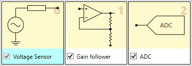
Suppose our sensor outputs 1 mVpp, and has a 100 kOhm resistance. We can set these parameters in the Sensor Stage Definition Panel. We’re going to ignore any inductance in this simple example.

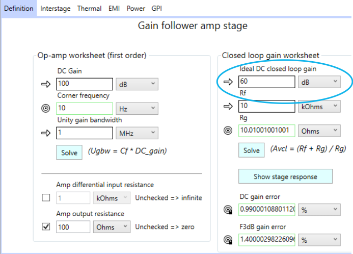
Using the Gain Follower Stage Definition Panel, we can set the amplifier stage to be non-inverting (that is, a “Gain follower”), having 60dB closed loop gain. We’ll use a 741-like op-amp. Here are the details:
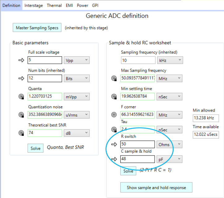
To end the analog portion of our signal chain, we’ll use a 5 V, 12 bit A/D having 50 Ohms switch resistance, and 48 pF sampling cap, as set in the lower right corner of the Generic ADC Definition Panel:
Let’s first determine the signal quality before turning on any “gargoyles” (gargoyles = EMI + connection parasitics). Pressing the Update button in the upper right panel computes the signal quality for us, as shown below. Note the Gargoyles! Check Box is turned off for the moment. Though we have no interference, we do have thermal and quantization noise which degrade the signal. These properties are modeled automatically for us and are given in the lower part of results panel:
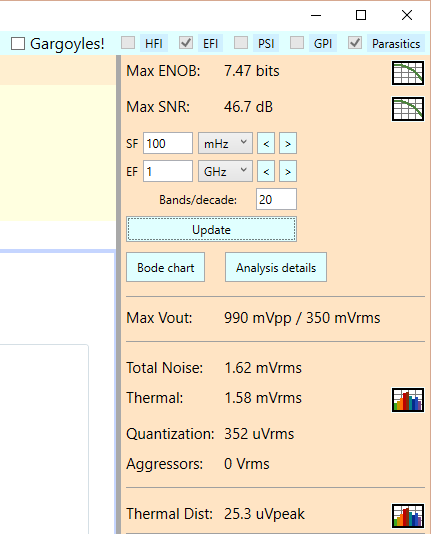
We end up with roughly 7.5 bits, so even though we have a 12 bit A/D, some of that resolution is being wasted. Our corresponding SNR is just under 47 dB.
Thermal noise dominates the signal degradation, coming in at 1.58 mVrms, whereas quantization noise is 352 uVrms. These are in comparison to a 350 mVrms (roughly 1 Vpp) output signal.
Though our 1 mVpp input signal has been amplified to 1 Vpp, we specified a 5 Vpp A/D. So we aren’t using the full range of the A/D, and we could improve things somewhat by either choosing a different A/D with a 1 V full scale, or by given the signal more amplification. But we’ll leave things as they are, for the effects of not using the full range are not significant in this example.
Adding Clock Line Interference
The results we just gave are the ideal ones — there is no outside interference, and no trace connection parasitics. In particular, we don’t yet have the 5 V, 1 MHz clock line interfering with our signal chain. Let’s put that in play by placing the clock line just 1 mm away from our signal traces. Here are the settings in the Master EFI Dialog that do this for us:

Since this is a “master” setting, it applies to each interstage connection — in our case, between the sensor and the amplifier stages, and between the amplifier stage and the A/D converter. Each of these connections are modeled the same: The EFI is injected as an “error voltage”, in this case 5V as per our setting above. The effective capacitance Ce is computed using the assumed geometry of the interference — the clock line trace is placed in parallel to the signal line trace, using a parallel plate capacitance model. We’ll study this model in depth in later articles.
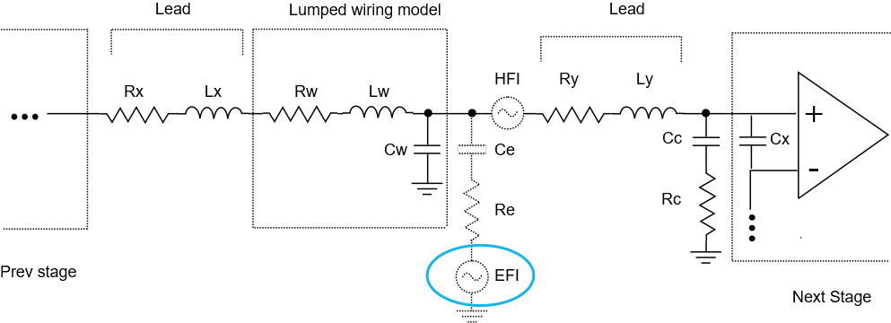
Here’s an example of the worksheet used to compute the effective capacitance of the clock-line-to-signal-line geometry:
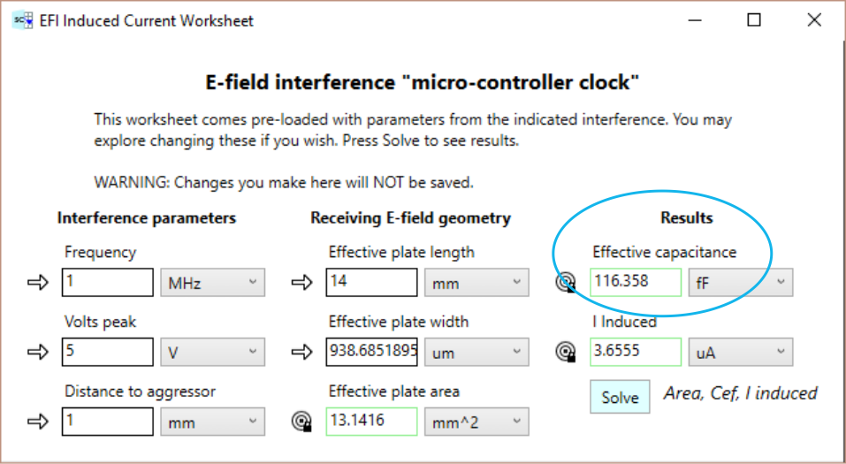
In computing the values, a master set of parameters is used for lead parasitics and trace geometries, etc, but these can be modified individually for each stage. For simplicity, we leave them the same for all the interstage connections of our example.
To enable the clock line interference, we must turn on the Gargoyle flag, the EFI flag, and the Parasitics (for the interstage connections) flag. We leave the HFI (H-Field interference), PSI (power supply interference), and GPI (ground plane interference) check boxes off. These checkboxes are located at the top of the main screen. Pressing Update gives us the new results: We see a drop from 7.47 ENOB to 1.89 ENOB, the SNR also dropping from 46.7 dB to just 13.2 dB.
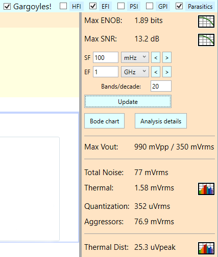
We’ve lost 33 dB of signal due to the pesky clock line. Inspecting the noise summary in the right side panel, we see that the aggressors (aka gargoyles) are now dominating the noise, contributing 76.9 mVrms of the 77 mVrms total. Popping up the Analysis Details Dialog, we can scroll down to the EFI section:

The EFI shows up in two places: S1 (before Stage 1), and S2 (before Stage 2). These interstage connection points default to having the same geometry as mentioned earlier, but the first has the biggest effect, because its interference is subsequently amplified 1000x by the amp stage.
Mitigating the Effects of the Clock Line
How do we control this interference? There are two easy ways: (1) By moving the clock line further away from the signal line, and/or (2) using a low pass filter.
Let’s do the first, moving the clock line various distances away. The following table lists the results:
| Distance | ENOB | SNR | Noise |
| 1 mm | 1.89 bits | 13.2 dB | 76.9 mVrms |
| 10 mm | 5.16 bits | 32.8 dB | 7.84 mVrms |
| 20 mm | 6.07 bits | 38.3 dB | 3.92 mVrms |
| 100 mm | 7.31 bits | 45.8 dB | 786 uVrms |
| 1000 mm | 7.47 bits | 46.7 dB | 78.6 uVrms |
These noise figures are in addition to the 1.58 mVrms of thermal noise and 352 uVrms of quantization noise. As we move the clock line further away, the thermal and quantization noise sources become predominant, so there is a point of diminishing returns in increasing the clock line distance. Not to mention, the latter distances, 100 mm and 1000 mm, are most likely impractical for most PCB scenarios. So we’d probably choose distances on the order of 10 to 20 mm, and these will get us within a few bits of the best answer we can achieve, given the signal chain configuration so far (7.47 ENOB).
We’d like to do better than this 7.47 ENOB, so how do we go about it? We can use the second method mentioned earlier, by incorporating a low pass filter. Let’s place one in front of the amplifier stage, and give it a corner of 1 kHz. (Thus we are assuming a signal slower than 1 kHz).
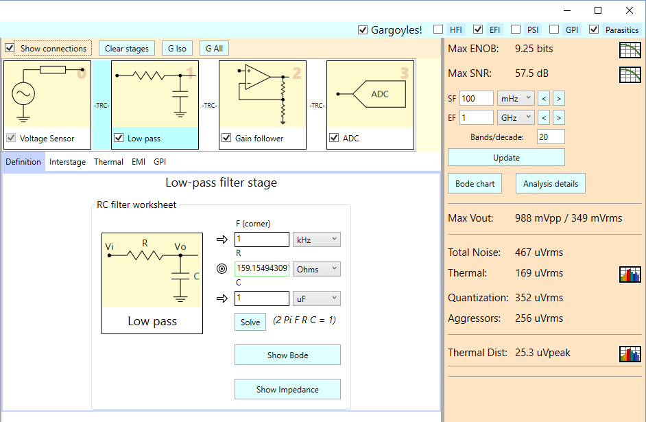
From the results panel, you can see we’ve improved the signal quality dramatically, from 1.89 to 9.25 ENOB, (13.2 to 57.5 dB SNR), an increase of 7.36 ENOB (44.3 dB). Remember, this is for the case when the clock line is 1 mm away.
By adding another stage, (the low pass filter), we’ve also added another stage interconnect, which by default is also susceptible to the global interference we’ve set — the 1 MHz clock line EFI. However, the capacitor in the low pass filter reduces this interference, both before and after the filter. The interconnect points are labeled as S1 and S2 in the following analysis details:

The EFI for these interconnects has been greatly reduced, down into nV territory. The S3 interconnect, between the amplifier and the A/D stages, hasn’t had its geometry changed, so it still has the same 256 uVrms noise it had before, but now it’s the dominant source of EFI.
We can experiment further by once again moving the clock line away, from 1 mm to 10 mm, for instance. If you do this and inspect the analysis details (not shown here) you’ll see that the clock line interference goes from 256 uVrms, to 25.6 uVrms, and we increase signal quality to 9.51 ENOB (59 dB). Note that as before, thermal and quantization still ultimately set the noise floor.
Conclusion
You’ve now seen the effects of a clock line placed too close to a signal line, in terms of EFI noise. We’ve shown how you can dramatically reduce these effects by moving the clock line further away. Sometimes you don’t have much room to maneuver in this regard, due to layout constraints, so a low pass filter might be used to further mitigate the noise.
For a 5V, 1 MHz clock line placed 1 mm away from our signal line, the following table shows how the initial signal quality drops, and then how you can gain that quality back by use of a low pass filter, and then move the clock line 10 mm away for even further gains:
| Environment | ENOB | SNR |
| no clock line | 7.47 bits | 46.7 dB |
| clock line 1 mm away | 1.89 bits | 13.2 dB |
| clock line 1 mm away, low pass filter | 9.25 bits | 57.5 dB |
| clock line 10 mm away, low pass filter | 9.51 bits | 59 dB |
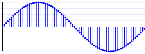
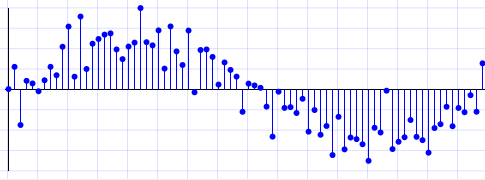
To give a visual indication of signal quality, below are plots of a sine wave with various amounts of SNR. These randomized plots were produced using the sister product, Signal Wave Explorer:
Clean sine wave:
13.2 dB SNR sine wave:
Sine wave with 59 dB SNR sine wave:
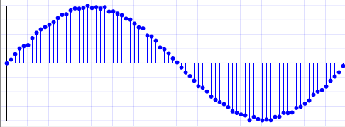
We think you’d agree the latter signal is much preferable. We also think you can now agree that paying attention to electric-field interference in your circuit is important, and Signal Chain Explorer can help you quickly get a handle on the magnitude of that interference. You can easily explore the system-level tradeoffs in your circuit.
Comments
Mitigating Clock Line Interference: Improving SNR by over 40 dB — No Comments
HTML tags allowed in your comment: <a href="" title=""> <abbr title=""> <acronym title=""> <b> <blockquote cite=""> <cite> <code> <del datetime=""> <em> <i> <q cite=""> <s> <strike> <strong>