Noise distribution considerations for a multi-stage audio amplifier
In this article we investigate how thermal noise and thermal distortion play a part in the design of a phono audio signal chain. For our example, we’ll use a Shure M97XE cartridge, a 47K/200pF termination shunt, three gain stages of 10X each, and then a 50 Hz low pass filter serving as a crude model for RIAA correction. We aren’t getting too detailed here in our design. The goal here is to see how the main sources of thermal noise play out. You’ll see that SCE can make quick work of such analysis.
NOTE: For a bit more refined example of using RIAA correction, see this blog post: Simple Digitized Audio Example.
Our Baseline
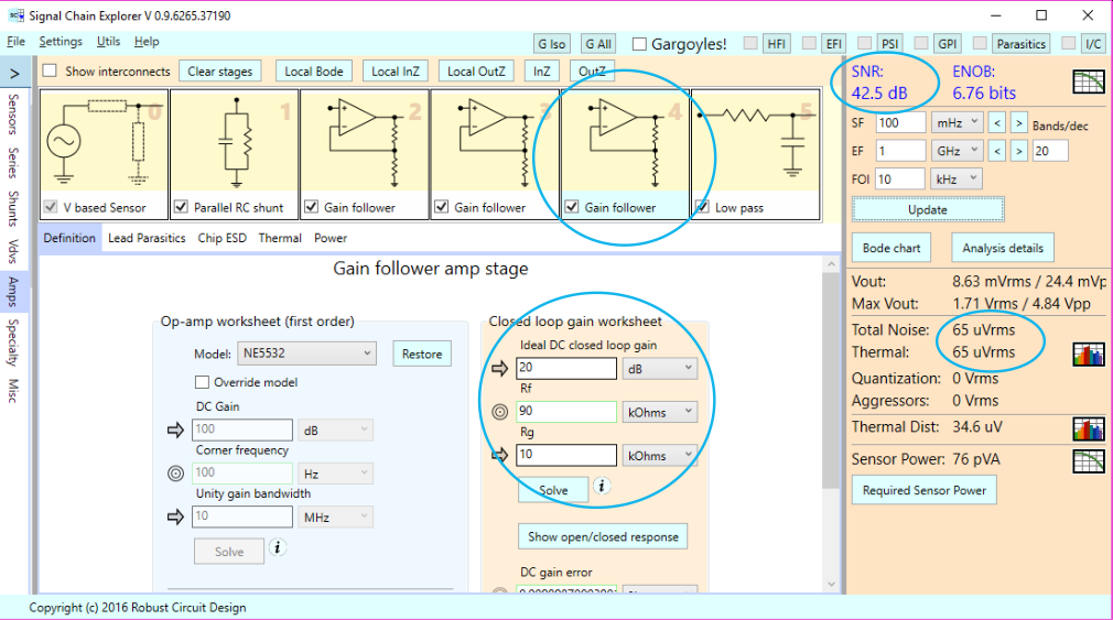
Okay, let’s see how we might set this up in Signal Chain Explorer. Below is the main screen, showing the signal chain at the top, and then the sensor (phono cartridge) stage definition. Note we’re using a nominal signal of 5 mVpp:
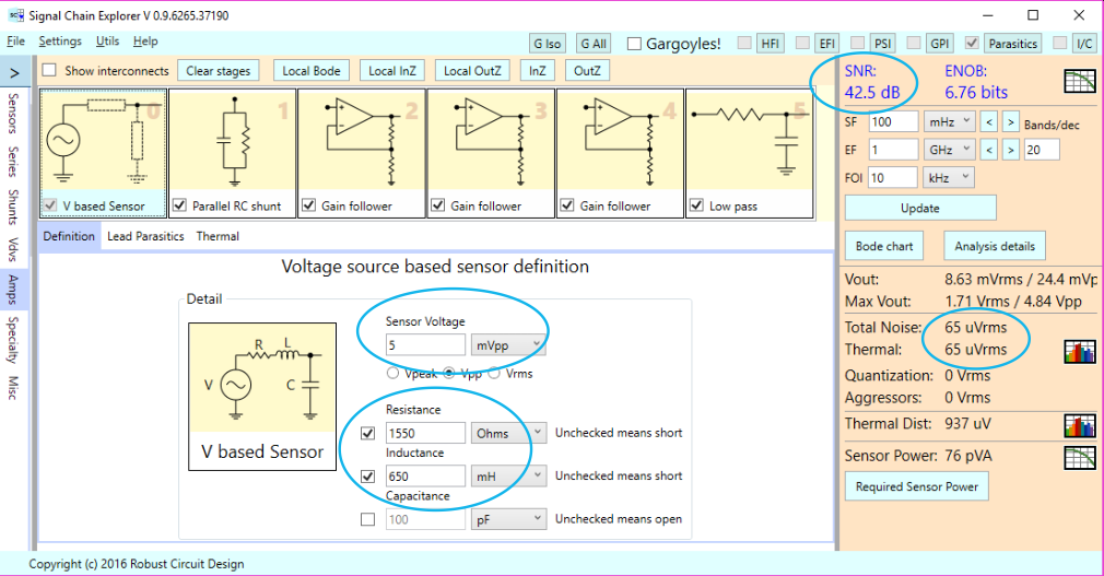
Baseline signal chain for phono audio amplifier
Overall, this signal chain gives us a gain of roughly 1000X, so our 5 mV input is converted to around 5 V at output (it’s actually 4.84 Vpp — slightly less than 5 V due to filtering roll-off), and we have an SNR of 42.5 dB — not great, but it’s a starting point. Our total integrated thermal noise is 65 uV. We’ll be seeing that in detail shortly.
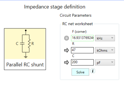
The termination shunt stage looks like the following. It’s purpose is to help control peaking that might otherwise be caused by the cartridge inductance, cable parasitics, etc.
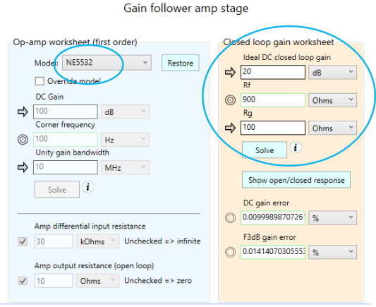
For our three amplifier stages, we’ve chosen to use NE5532 op-amps, (which have 5 nV/rootHz of thermal noise) and have set up the stages identically for 20dB each, using feedback resistors (Rf) of 900 Ohms, and resistors-to-ground (Rg) of 100 Ohms:
 |
 |
With a lack of knowledge of any other constraints to the contrary, using equal gains for the stages is a reasonable strategy to start with. Using the same components for each stage also helps keep the parts list under control. We’ll soon see whether this is a good strategy.
Baseline Results
Okay, with all these definitions in place, let’s look at the resulting thermal noise plot (obtained by clicking the thermal noise icon in the lower right panel of the main screen):
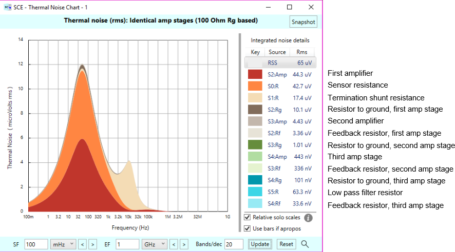
SCE’s stacked thermal noise plots are invaluable. They can tell you a lot in a quick glance, both graphically and numerically. (See this post to understand how to interpret the charts in detail). The main thing to notice here is that the op-amp in the first amplifier stage (Stage 2, hence “S2:amp”) dominates the noise, coming in at 44.3 uV, followed closely behind by the noise in the sensor itself (S0:R) of 42.7 uV, and then the termination shunt resistance (S1:R) noise of 17.4 uV. The rest of the noise sources fall off quickly from there. These observations help you understand a few of the main rules of thermal noise design in signal chains:
- The first op-amp often dominates the noise. It behooves you to use a low-noise amplifier there if you can. Our NE5532 op-amp is decent, but there are op-amps available with much lower noise. You can get down to the 1 nV range, (instead of the 5 nV the NE5532 has.)
- The sensor noise also is a main contributor, it might even be the biggest. There’s not much you can do about it, except try to use a lower-noise sensor or one with a stronger signal. If this weren’t an audio signal chain, you might get away with a low or high or bandpass filter in front of the first amp stage to help get rid of sensor noise, depending on the type of signal you’re dealing with.
- The third rule has to do with a tradeoff between thermal noise and thermal distortion, which we’ll get to in a bit.
First Op-Amp Often Dominates
Why does the first op-amp noise dominate? Because, along with the sensor, its noise gets amplified the most, passing through all the gain stages. In our 20 dB gain stages, the op-amp noise of the first stage gets amplified first by a noise gain of 10X, then by 10X again by the second amp stage, and then by 10X one more time by the third op amp stage, for a total of 1000X. Hence, the first op-amp has ten times the overall output noise than the second op-amp, which has 10 times the overall output noise of the third op-amp. You can see this progression clearly in the right-hand data panel of the thermal noise chart, which we’ve isolated and annotated below:
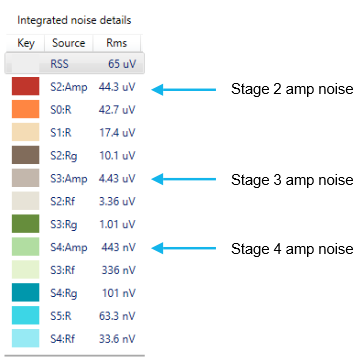
See how the amp noise contributions are 44.3 uV, 4.43 uV, and 443 nV, respectively, going down a factor of ten each time, even though the amplifiers are identical in spec.
Because the amp noise contributions fall off rapidly (depending on the gains of the stages — the more gain, the faster the relative subsequent amp stage noise contributions fall off) you can take advantage of this by using as low a noise op-amp as you can in the first amp stage, and then relax your noise standards for the other amp stages. These stages can have much higher op-amp noise without affecting the overall signal chain noise, so you can use cheaper parts, or perhaps op-amps with better slew-rate, distortion, or power specs.
The same progression is true for the resistors in the amp stages — each subsequent stage amplifies the resistor noise of the previous stages. In our example with stage gains of 10X, the resistor noise contributions also fall off by a factor of 10 at each stage. Below is our thermal noise chart data panel annotated for the Rg resistors:
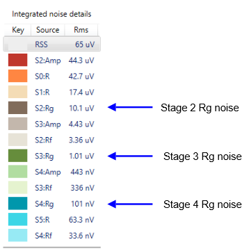
A similar reduction-by-ten pattern holds for the feedback (Rf) resistors.
Thermal Distortion Rears Its Ugly Head
You might wonder, then, why not use higher value resistors in the later stages? Turns out, that’s probably a good thing to do. As the signal passes from one gain stage to the next, the voltage swings get bigger and bigger, and this causes in turn larger and larger current swings. Larger current swings means greater distortion from the op-amps, both in terms of non-linear distortion — and in terms of thermal distortion. The resistors are also affected by the greater currents, which cause more heating and thus more thermal distortion.
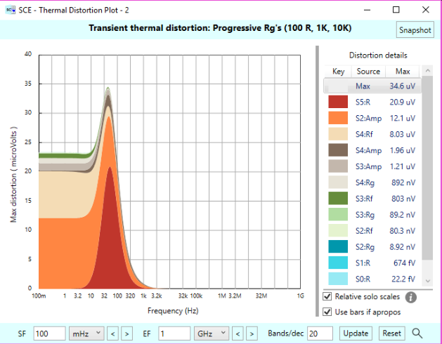
Let’s take a look at the thermal distortion in our signal chain. Below is such a plot, generated in SCE by clicking the thermal distortion icon in the lower portion of the right hand panel of the main screen. The thermal distortion plot is similar in look and feel to the thermal noise plot. For each op-amp and each resistor in the signal chain, SCE looks at the maximum current amplitudes through the devices and estimates the amount of heating and subsequently, the amount of voltage distortion:
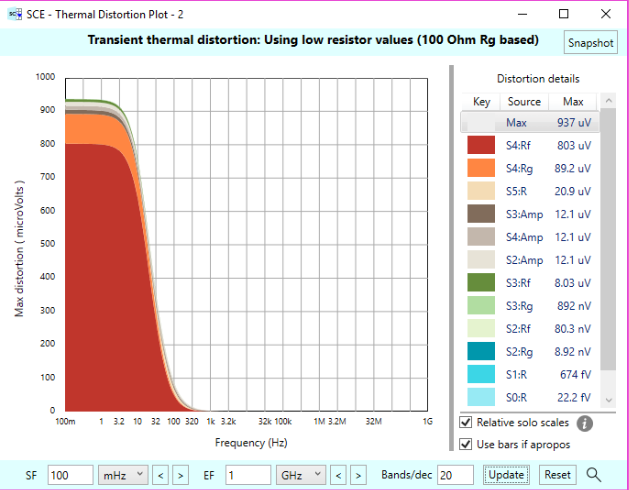
First thing to notice is a whopping amount of distortion at low frequencies — in this case, around 900 uV. This is in contrast to the 65 uV of thermal noise. (Note: The former is in Vpeak, where the latter is in Vrms.)
NOTE: We must point out here that SCE is giving you a worst-case estimate. The program pretends that all the voltage or gain offsets caused by thermal heating are combined in the worst way possible — their absolute values are simply added up. No allowance is made for offsets that might cancel each other out. For example, in a well designed system, the Rf and Rg resistors in an amp stage would be placed next to each other in the same thermal environment. Thus, their thermal distortions would rise and fall together, and the subsequent gain produced by their ratio would stay relatively unaffected. If these two resistors are in different thermal environments that wouldn’t be the case, and gain errors would accrue. SCE assumes this latter case.
Now, this maximum distortion is occurring mostly in the sub-audible range — from DC to around 10 Hz. So you might think this would not be a problem. The trouble is, those low frequency voltage offsets will alias with the higher frequency audio signals due to intermodulation distortion, which will appear at audible frequencies.
Tradeoffs Abound
So it would seem we should use higher value resistors. The problem is, the higher the resistance, the more thermal noise. Hmm… And didn’t we just say a bit ago, the lower the resistance, the more thermal distortion! These two rules are opposing each other. We can’t win!
Yes, there is a tradeoff occurring here. But remember, the later the stage, the less effect its relative noise contributions have on the overall thermal noise. So we can afford to use higher value resistors for those. And that’s a good thing, because that’s where the voltage swings — and hence the danger of more currents and thermal distortion — occur.
A Possible Strategy
What resistance distribution pattern should we use? Well, without any other information to the contrary, you could try using progressively higher resistor values as we go through the stages, perhaps, in our example, by allowing each stage to have resistances ten times higher than the previous stage. For example, our first stage can have, say, 100 Ohms, the next stage, 1k Ohms and then the third, 10k Ohms. The exact numbers to use could be obtained from, say, a signal chain optimization program — and we here at RCD have been investigating just that. But for now, we’ll stick with our 10X progression. Below is the result of putting this into play:
Here, we are showing the last stage’s definition in the main panel. Notice Rg = 10k, and to keep the gain at 20 dB, we correspondingly set Rf to 90k. The following table shows the resistance distributions of all three amp stages. (And note we’ve left the amplifier noise figures at 5 nV/rootHz for each stage. We could have relaxed those as well.)
| First amp stage | Rg=100 | Rf=900 |
| Second amp stage | Rg=1k | Rf=9k |
| Third amp stage | Rg=10k | Rf=90k |
From the results panel, you can see the overall noise is at 65 uVrms — just like it was before. (It has changed in the lower significant digits, which we can’t see in our formatted output.) But the max thermal distortion has plummeted — from around 900 uV, to just 35 uV.
Let’s look at these error sources in more detail. Here’s the thermal noise plot, using our Rg=100, 1K, 10K based sequence:
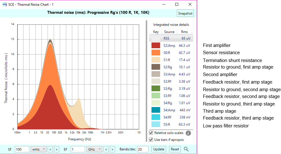
The noise contributions of the resistors in the later stages have gone up, but they haven’t really affected the overall result.
NOTE: In case you’ve forgotten, the thermal noise contributions are not merely summed up — they are root-sum-squared. Thus, the higher contributors will dominate the show. The lessor contributors can be changed in apparently significant ways (in this case, up by factors of ten) without causing much effect.
The thermal distortion plot shows where we’ve won — by dramatically lowering the worst case voltage offsets, from 900 uV to just 35 uV:
Gargoyles Lurk!
Our worst case thermal distortion voltage offset is still relatively high — 35 uVpeak as compared to the thermal noise of 65 uVrms. So you might think, “Hey! Why not make the resistors in the later stages even larger!”
You could do that, and in terms of reducing thermal distortion, that will work to some degree. But there is a danger lurking there. If you make the resistors too high, they will begin to interact with the pin parasitics of the op-amp chips, and might cause peaking.
Let’s see this in action, using SCE. Just a few clicks will get us there. First, let’s change the last stage’s Rg value to 1 MOhms, (and subsequently Rf to 9 MOhms). Next, let’s change the op-amp to something with a higher unity gain bandwidth. The NE5532 has a UGBW of 10 MHz. Let’s choose the OPA211, which has a UGBW of 45 MHz. Here’s the modified stage definition for the last stage:
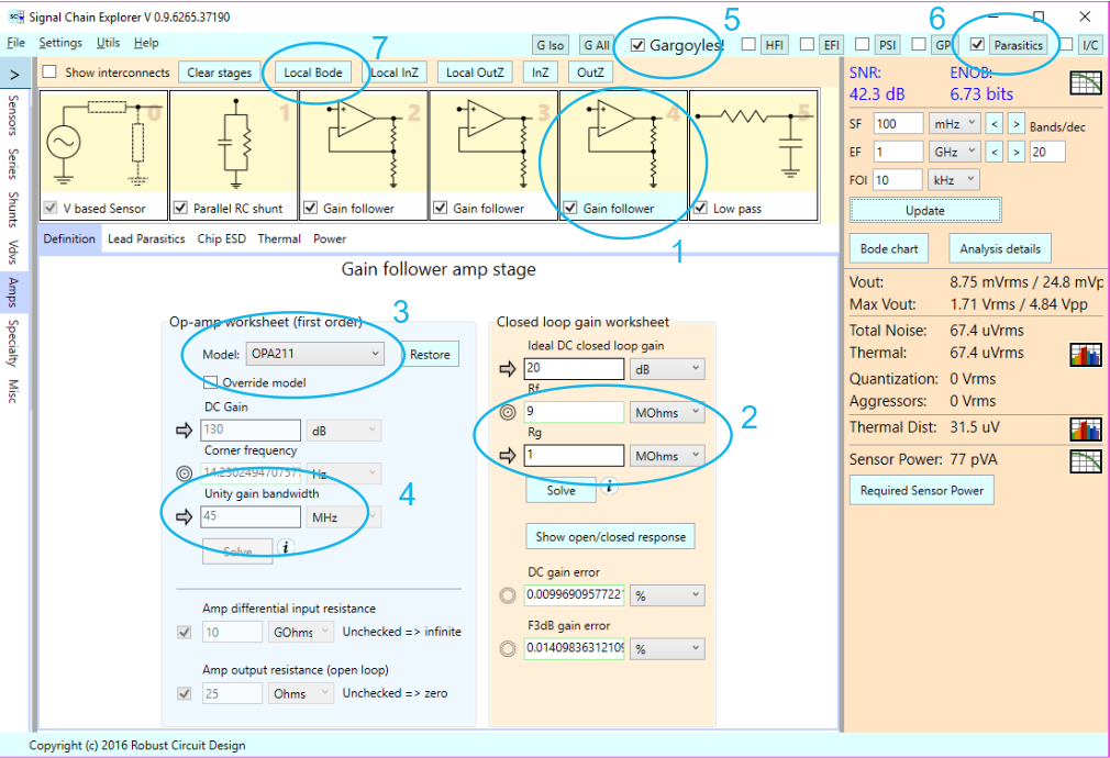
The next steps are to turn on the chip parasitics. To do this, first check the Gargoyles! toggle located at the top of the main screen, as shown in the above figure. Then turn off all the individual gargoyles except for Parasitics, also shown above. By parasitics we mean chip ESD structures on the input pins. With these settings in place, be sure the last gain stage is selected as shown above, and then click the Local Bode button. Here’s the resulting plot:
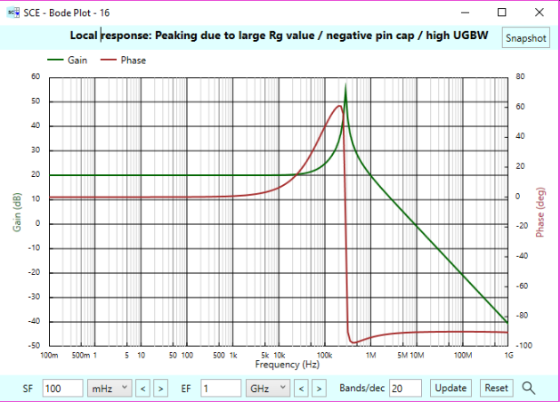
You can see prominent peaking out at 300 kHz. This peaking is caused by a combination of: (1) High Rg value of 1 MOhm interacting with 2 pF capacitance on the negative pin of the op amp, and (2) a high UGBW of 45 MHz. If you were to lower the UGBW to say, 10 MHz, this peaking would be greatly reduced, if visible at all. The reasons that these things interact the way they do will be the subject of another blog post (we hope.) Note that we don’t fully understand this phenomenon ourselves, but predicted the resistance-capacitance interaction. The UGBW interaction needs further study.
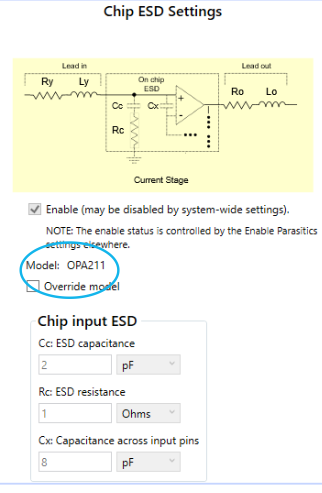
Just to be clear about the pin capacitance, here’s the Chip ESD Settings for the OPA211. What we call Cc below is the value used for both the positive and negative input pins. Here, it’s 2 pF:
Summary — Rules for Distributing Noise Sources
In this article you’ve seen how thermal noise and thermal distortion interact in a multi-stage amplifier signal chain. In summary, here are the things to keep in mind when designing for noise and distortion mitigation:
- Being the first stage, the sensor is often a big contributor to the overall noise. It’s hard to control it, in general. You get what you get. If you’re lucky, you can use a filter of some kind to keep the noise at bay.
- The first op-amp stage is critical for keeping noise down. Use as low-noise of an op-amp as you can get away with. Use small values for the resistors as well.
- For the later stages, you can relax the low-noise requirements on the op-amps, and you can use higher resistor values. You can progressively allow higher and higher noise contributions in the subsequent stages because their overall contributions will be relatively small compared to the early stages.
- There is a trade-off between thermal noise and thermal distortion. Pay attention to both. Thermal noise is more a problem in the earlier stages. In contrast, thermal distortion is more of a problem in the later stages, due to higher voltage (and thus current) swings. You want higher resistances there to keep the currents down.
- Beware of making the resistance values too high. The large resistances can interact with pin parasitics and cause peaking.
Comments
Noise distribution considerations for a multi-stage audio amplifier — No Comments
HTML tags allowed in your comment: <a href="" title=""> <abbr title=""> <acronym title=""> <b> <blockquote cite=""> <cite> <code> <del datetime=""> <em> <i> <q cite=""> <s> <strike> <strong>