SCE Lesson 1 – Building and Analyzing Your First Signal Chain
Introduction
The main purpose of Signal Chain Explorer’s (SCE) is to quickly build a signal chain and explore how interferers degrade the signal to noise ratio. With that in mind, in this lesson we’ll build a simple signal chain and see how SCE can compute, at the push of a button, the signal to noise ratio, which is affected by signal strength, quantization noise, and thermal noise.
TIP: If you haven’t read the SCE Quick Tour document, now is the time to do so, as that document gives you a good overview of SCE. Also, it’s highly recommended you familiarize yourself with SCE’s unique Unit Var Fields and Equation Worksheets as they are key to using the product.
In the following discussion, we’ll be using these features without giving much detail as to their operation. So be sure to review the two documents above before starting this lesson. The preceding links will take you to these pages.
Now, on to your first real lesson!
Step 1 – Start a New Signal Chain
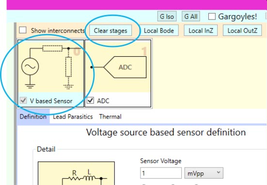
Start up SCE, or if you’ve already been using it, click on top center Clear Stages button to start a new signal chain. You’ll see two stages appearing by default in the signal chain panel: A “V based Sensor” stage and an “ADC” stage.
Step 2 – Edit the Sensor Stage
Click on “V based sensor” stage icon to ensure the stage is selected. You can tell because it will have a cyan label at the bottom of the icon, as opposed to a white label. Once selected, you can edit the stage using the Voltage source based sensor definition panel that appears in the center of the main screen. There are multiple views in the stage definition, which you can switch to using horizontal menu at the top of the stage definition. For now, ensure the Definition tab of the stage definition (in the middle panel) is selected.
<Figure 1>
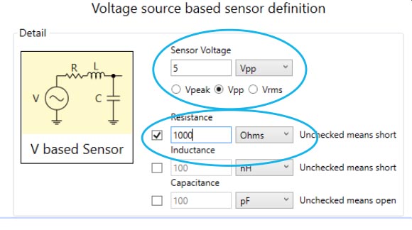
In the Sensor Voltage field, type in “5e3”. (Note the default scale is mVpp as shown in the combo box to the right of the edit field). Press Enter. SCE automatically changes the value to 5 and updates the combo box to show Vpp. So we now have 5 Vpp as our sensor signal. The way to think of this value is to pretend that it’s the sensor’s voltage for all frequencies of analysis. Of course, if the sensor has impedance (most will), the actual voltage at the output of the sensor stage will be different, and may in fact vary by frequency.
<Figure 2>
By default, the voltage sensor stage is “ideal”, having an ideal voltage source with no impedance. You can add impedance via the series Resistance and Inductance fields that default to disabled (meaning they act like a short.) Now enable the Resistance field by checking the box to the left of the field and edit its value to be 1000 ohms. Leave the inductance disabled.
You can also define a capacitance to ground as controlled by the Capacitance field below the other two. Let’s leave that field disabled, (which means the path to ground is “open.”)
The upshot of all of this is that we’ve now defined a sensor to have a voltage source of 5 Vpp, and a series impedance of 1000 ohms.
Step 3 – Set the System Analysis Parameters
The main result computed by SCE is the Signal to Noise Ratio (SNR) and Effective Number of Bits (ENOB). In order to compute these values, you must first define the frequency range you’d like covered, as these values depend on that range. For example, the wider the range, the more thermal noise — which is the often the main noise source and thus is what drives the SNR (and ENOB) down.
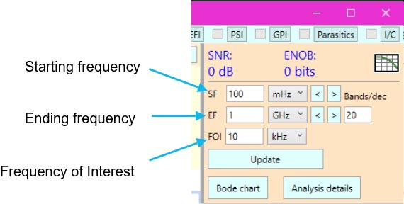
The frequency range is defined by two fields in the upper right panel (the main Analysis Panel): The starting frequency (SF), and ending frequency (EF). These default to 100 mHz (0.1 Hz) and 1 GHz. For now, ensure these values are set.
<Figure 3>
Another critical field that affects the results is the Bands/Dec (bands per decade). This controls the resolution of the simulation and the plots. It defaults to 20 bands/dec, which means in each power of ten range, 20 sampling points are used. For example, there are 20 points between 100 mHz and 1 Hz, 20 between 1 Hz and 10 Hz, 20 between 10 and 100 Hz, and so on. Ensure the default value of 20 bands/dec is used for now.
The last critical field to set is the Frequency of Interest (FOI). This is the frequency used when reporting many of the values in the analysis panel — such as SNR, ENOB, voltage out, sensor power, etc. Ensure the default value of 10 kHz is set for now.
Step 4 – Run Your First Analysis
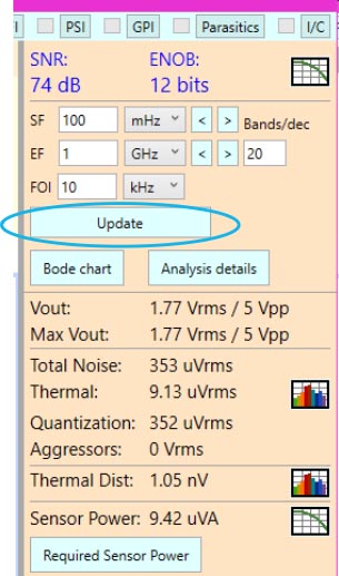
An analysis is run by clicking the Update button located prominently in the upper portion of the Analysis Panel.
<Figure 4>
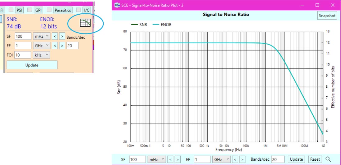
You should see the SNR field update to 74 dB, and ENOB to 12 bits. As a reminder, these are calculated at the frequency of interest (FOI)– in our case, 10 kHZ. You can optionally see a plot of these values vs frequency by clicking the graph icon to the right of the ENOB field.
<Figure 5>
While this graph shows both SNR and ENOB labeled with green and cyan lines, the cyan ENOB plot lines may hide the green SNR plot lines. That’s the case here. Note, though, that their units and scales are different as indicated by the different Y-axes left (for SNR) and right (for ENOB).
If you’ve opened this graph, close it now (using the upper right X button) to continue with this lesson.
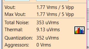
Listed below the Update button are other important results of analysis: Here, out output voltage (at 10 kHZ FOI) is 1.77 Vrms (or 5 Vpp). Total noise is 353 uVRms. You can confirm the calculation of SNR from these two numbers: 1.77 Vrms / 353 uVrms — roughly a ratio of 5000, or 74 dB.
<Figure 6>
Below the total noise field is a summary breakdown of where that noise comes from. In our case, there are 9.13 uVrms of thermal noise, (set by the resistors in the circuit and the frequency range) and 352 uVrms of quantization noise (set by the sampling resolution of the A/D converter.) So in this case, the quantization noise dominates.
Step 5 – Inspecting the System Bode Chart
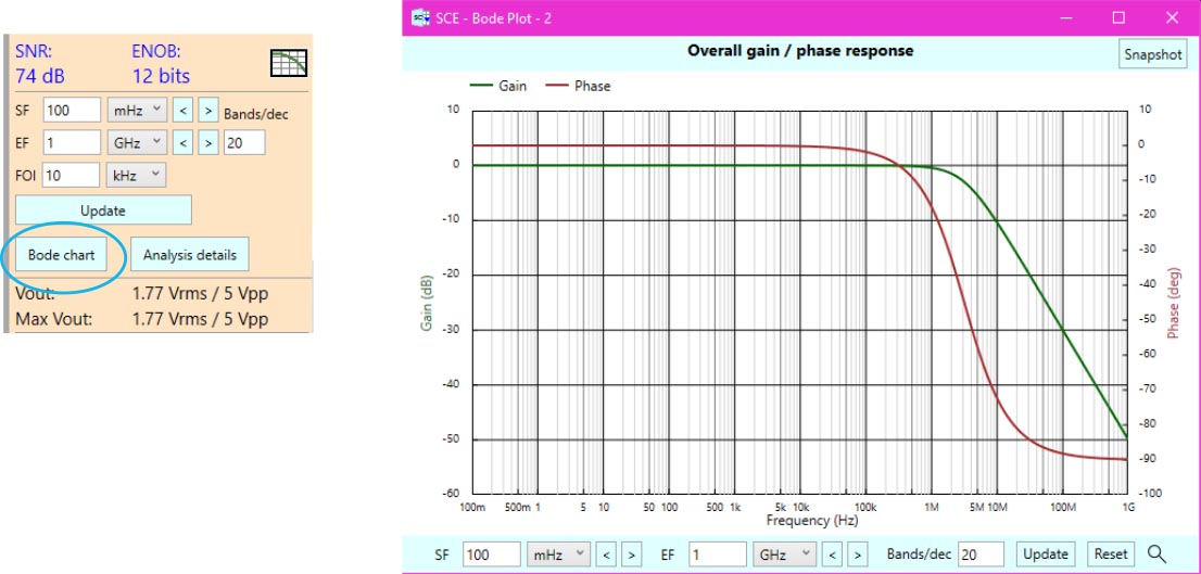
One other result you’ll likely want to see is the gain/phase chart. Click the Bode chart button just below the Update button to see this plot appear.
<Figure 7>
Notice the gain plot (green line) is flat (at roughly 0dB) sloping ever so slightly out to 1MHz, near the f3dB corner, and the drops dramatically from there in 20db/decade, down to -50dB by 1GHz. Notice the red phase plot crosses 45 deg right at the f3dB corner.
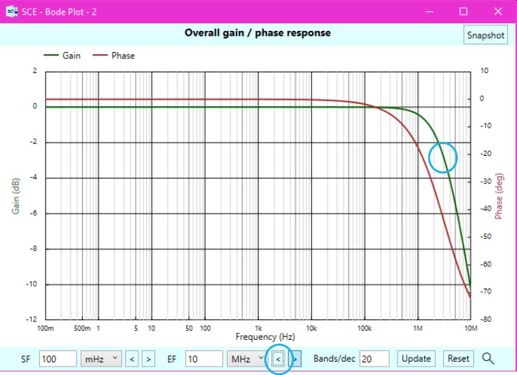
We can get a better idea of where the corner frequency is by zooming in on the plot. There are two sets of “<, >” button pairs at the bottom of the graph that help in this regard. These change the starting and ending frequency, respectively. In each pair, the “<” button reduces the affected frequency boundary, the “>” increases it. To zoom in properly, you’d increase the starting frequency (using the “>” button in the SF section), and decrease the ending frequency (using the “<” button in the EF section). Use the opposite buttons to zoom out.
NOTE #1: These changes in frequency range are for the chart only, and do not affect the system frequency range as given on the main screen.
NOTE #2: When zooming in, SCE actually recalculates the data points, using whatever resolution you have selected in the Bands/Dec field. It doesn’t just re-plot the same old points. By increasing the resolution, you can zoom in to arbitrarily small ranges of frequencies, looking for sharp peaks, for example. To change this resolution temporarily for this chart only, edit the Bands/Dec field, and then press the Update button on the chart dialog.
For example, to zoom in, let’s simply change the ending frequency EF by clicking twice on the appropriate “<” button to the right of the EF field. Each click reduces the ending frequency by a power of ten, so two clicks reduces the 1 GHz frequency to 10 MHz. Now it’s easier to see the f3dB corner frequency on the chart — it’s near 3 MHz.
<Figure 8>
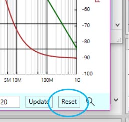
Sometimes after using the zoom buttons you can get the chart so messed up it’s hard to figure out where you are. The Reset button on the lower right comes to the rescue in cases like this. This button resets the frequency range of the chart back to the system frequency range as given on the main screen. In our case, that’s 100 mHz and 1 GHz. Click Reset to see this change take effect.
<Figure 9>
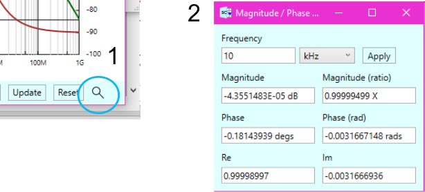
The other button of interest on this chart is the Inspect button (having a search icon) on the extreme lower right. This pops up a dialog showing details at any frequency you choose, as related to the current chart. It defaults to the frequency of interest. In our case, at a FOI of 10 kHZ, we have a gain of -4.4 dB, and phase of -0.18 degrees.
<Figure 10>
You can change to any frequency you want and then press Apply to see the values at that new frequency, but note that this does NOT affect the system FOI in any way. It’s only for the current chart.
Close this dialog — and the Bode chart — to continue with the lesson.
Step 6 – Introducing the ADC Stage
If you were paying attention to the Bode chart, you’ll notice that our system has classic low-pass behavior. But where does that behavior come from? It’s due to the low-pass filter that’s formed by the resistance in the source stage, and a resistor-capacitor voltage divider in the ADC stage. Next, we’ll take a closer look at the ADC stage to see what’s going on. Then, in later steps, we’ll play around with the sampling resolution and the sampling capacitor value, as these two things can have major impact on the system’s SNR.
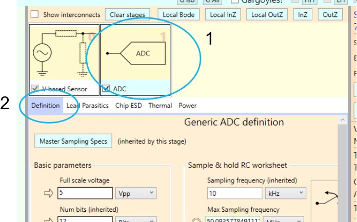
To see the A/D parameters, click on the ADC stage icon in the signal chain list in the top panel. The bottom portion of the stage’s icon turns cyan, and the stage definition appears below it in middle panel of the main screen. Ensure the that the Definition tab is selected in that middle panel.
<Figure 11>
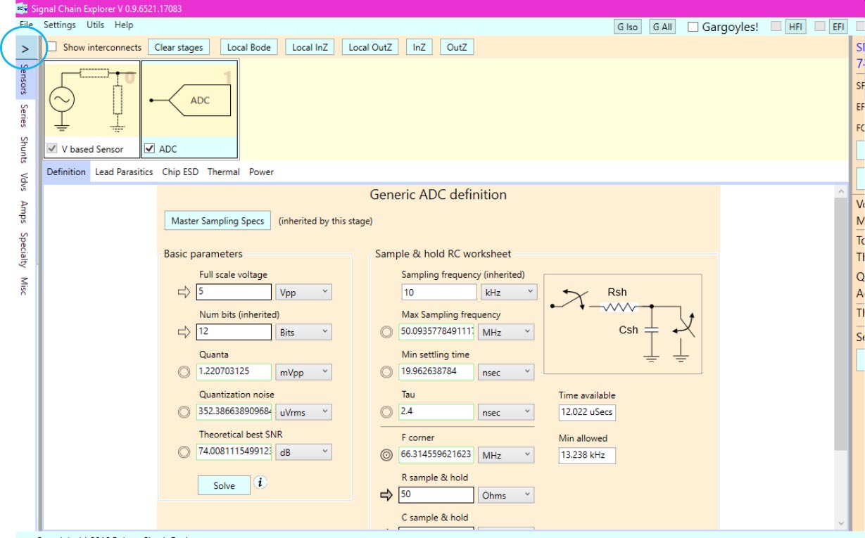
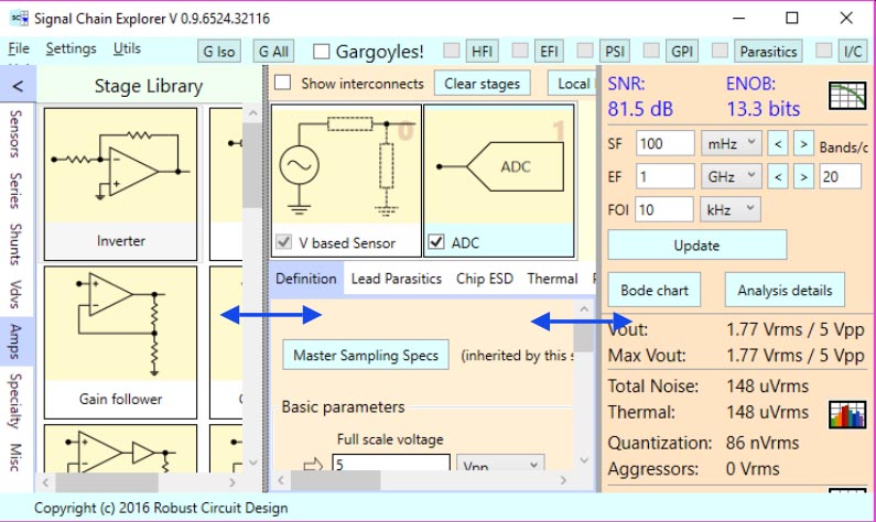
You may not be able to see all of the stage fields. You can use the scroll bars provided for the panel to scroll them into view, or one quick way to solve this problem is to collapsed the left-side Stage Library Panel by clicking on the chevron toggle on the upper left side, just below the menu. This collapses the panel to give us more room for the middle pane. Clicking the chevron again restores the left panel. Each press toggles this behavior.
<Figure 12>
You can also adjust the widths of the left and right panels by dragging the two vertical gray bars that separate the panels from the middle panel.
<Figure 13>
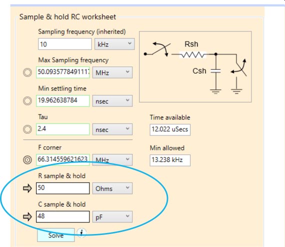
With the ADC panel in view, notice the diagram at the top right. This illustrates the high level workings of the A/D: It’s a sample-and-hold circuit with a series resistance and a cap to ground.
<Figure 14>
This switched voltage divider acts like a low pass filter. In our case, the switch resistance defaults to 50 ohms, and the cap to 48 pF. This sets the low-pass corner of the switch to roughly 66 MHz. Many of the fields on the right side panel of the ADC stage definition concern this value, and there’s way more to say about this, but we’ll leave that for another lesson. For now, know that the 50 ohm resistor combines with the 1000 ohm resistor in the source stage, to give our system a total of 1050 ohms of resistance. With the cap to ground set at 48 pF, this gives our overall system (as opposed to just the ADC) a corner frequency of around 3 MHz. You saw that in the Bode chart in the last step.
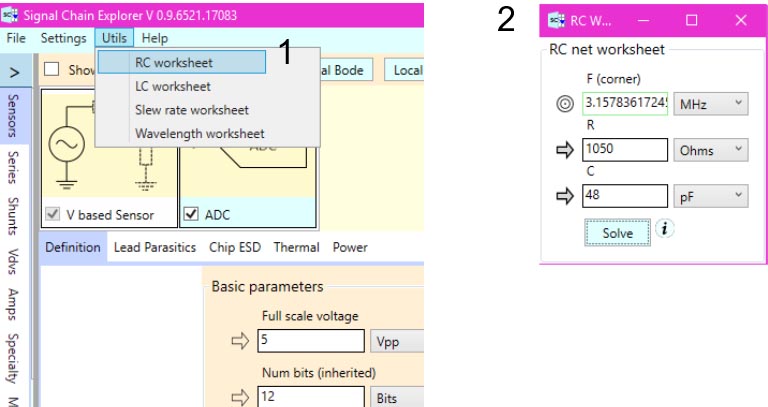
There’s an easy way to double-check this math right in SCE. In the Utils Menu located on the main menu bar you can invoke the RC worksheet.
<Figure 15>
The worksheet that pops up let’s you enter a resistance and capacitance and then calculate the f3dB corner by clicking the Solve button. In the case here, we get a corner of 3.1 MHz, which confirms the result. Close this dialog to continue.
So that explains the low-pass behavior of our system. But what about the other main behavior, that of the SNR, and in particular the noise in the system?
Step 7 – Changing the Sampling Resolution
You saw earlier that the noise in our example is overwhelmingly dominated by quantization noise — which comes straight from the parameters of the ADC, in particular, its bit resolution. You can see in the left worksheet of the ADC stage panel that we’ve defaulted the ADC to have 12 bits of resolution.
There’s a formula that gives us the quantization noise versus bits of resolution, but that’s outside the scope of our discussion here. Just note that this formula gives us 352 uVrms of noise as seen in a field lower down in the worksheet. That noise in turn leads us to a theoretical best SNR — that is, the most we could ever hope to achieve in an ideal situation — of 74dB (shown below the quantization field.) We’ve seen these numbers before — the roughly 352 uVrms of noise, and the 74dB SNR on the main analysis screen. So our system is close to “ideal” — at least for a 12 bit system.
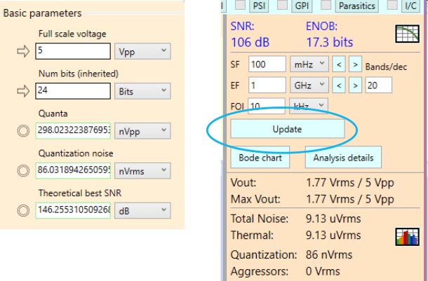
Given that the quantization noise dominates our system, we could improve things quite dramatically by lowering the quantization noise, and we can do that by using a finer ADC resolution — say 24 bits instead of 12.
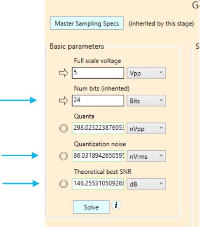
You can’t change the bit resolution directly in the ADC stage definition panel since it’s an inherited system value. Instead, you can click the Master Sampling Specs button in the upper left corner of the panel. This pops up the Sampling Worksheet dialog.

<Figure 16>
NOTE: This worksheet is also available from the Settings sub-menu of the main menu at the top of the main screen.
There is much to discuss about this worksheet, but that’s left for another lesson. Here, we’re only concerned with changing the bit resolution from 12 to 24 bits. Change the appropriate field in the middle part of the worksheet, and press Save the button on the lower right of the dialog. This will update the bit resolution in the ADC stage definition as you can see if you go back to the ADC stage panel. You’ll see now that the theoretically best resolution jumps to 146 dB.
<Figure 17>
At this point in time, our overall analysis panel is still showing 74 dB SNR, but since we’ve changed the resolution of the ADC, you can click the main Update button of the system and update the results: SNR is 106dB, ENOB is 17.3 bits, quantization is 86 nVrms, and the thermal noise remains at 9.13 uVrms.
<Figure 18>
You might wonder, why 106 dB SNR instead of the theoretical best 146 dB? While we’ve lowered the quantization noise to nanovolt levels, the thermal noise has stayed the same, and is now the dominate culprit preventing us from having a better SNR.
Step 8 — Inspecting the System Thermal Noise Plot
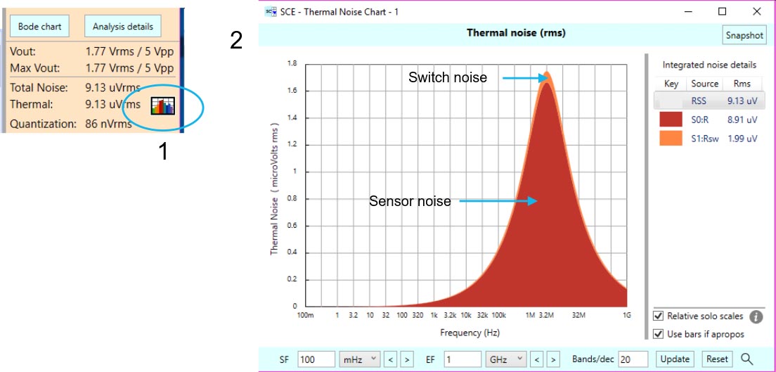
Speaking of that thermal noise, you can take a closer at its composition by examining the thermal noise plot, which can be invoked by clicking on the bar chart icon to the right of the thermal noise field in the main analysis panel.
<Figure 19>
You’ll see that the thermal noise is plotted vs frequency, and that we have two noise sources whose contributions are stacked on top of each other in the chart, given different colors. Here, we have the noise of the 1000 ohm resistor which dominates — it’s 8.91 uVrms of the 9.13 uVrms integrated total. The 50 ohm switch resistor in the ADC contributes roughly 2 uV of noise. You should note that these noise sources, being treated as random, are root-sum-squared together and integrated over the entire system frequency range to give the 9.13 uVrms total.
The thermal noise plot of SCE are one of its main features, and is quite unique to the product. A lot of insight can be gleaned from this chart. For a more detailed discussion of how to use this chart and how its data is computed, see the blog post Understanding Thermal Noise Charts in SCE.
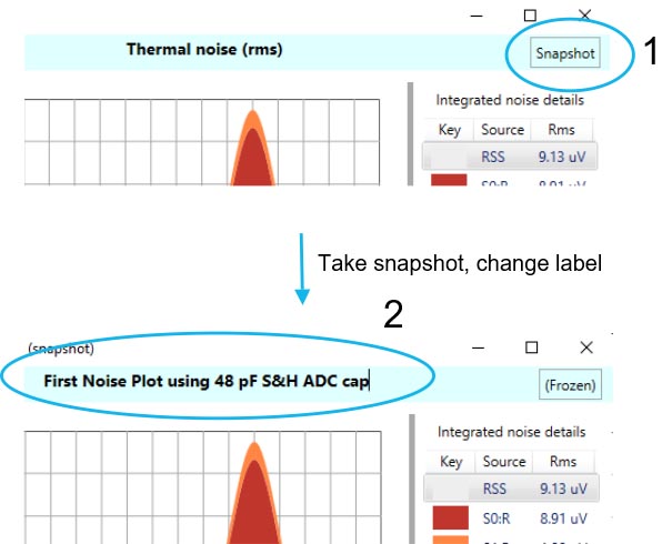
Once you’ve viewed this chart, you can close it using the X button at the top right corner, or, you can make a “snapshot” of its contents to be viewed later. Let’s keep the dialog open so that now so we can come back to it in a bit, and compare the results to a new chart generated by changing a few of the signal chain parameters.
To make a snapshot, click the SnapShot button on the upper right of the dialog. The button’s caption now changes to “Frozen” and you can then leave the dialog open, moving it out of the way if need be. You can also optionally edit the chart’s title (just click on the title and start editing) to give it a more descriptive name. For example, let’s make the title, “First Noise Plot using 48 pF S&H ADC cap.” You’ll see why we do this in a bit.
<Figure 20>
Step 9 – Improving ADC Response by Changing the Sampling Capacitor
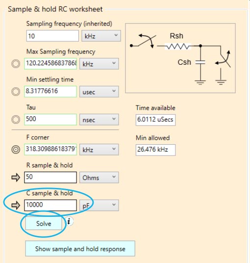
While the ADC model we use in SCE is generic and relatively simple (modeled as a sample and hold switch), we can model some of the behaviors of more sophisticated ADC’s, such as delta-sigma ADC’s — well, at least one of the significant features: The capacitor will likely be higher than our default 48 pF. In fact, let’s make it 10,000 pF. Change the field by typing “10000 pF” and press Enter (or click the worksheet’s Solve button.) The fields of the worksheet are appropriately updated.
<Figure 21>
Notice in particular that the ADC’s corner has dropped from 66 MHz to just 318 kHz. This lowering of the ADC corner will have a major impact on the system’s overall response. You can see that by clicking the Bode chart button to pull up the Bode chart, and notice the overall system’s corner has dropped from 1 MHz to around 15 kHz. (You can use the zoom “<,>” buttons of the Bode chart to home in on this.)
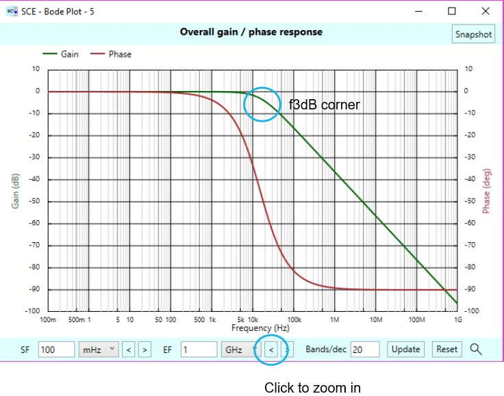
<Figure 22>
Lowering the corner of the system has one advantageous side-effect, it lowers the overall noise of the system because, with the lower corner, more high frequency noise is filtered out. You can see this by inspecting the main analysis panel (click Update just to make sure the values are updated.) Our SNR has risen from 106 dB to 127 dB, our ENOB to almost 21 bits. These large increases are because the thermal noise has dropped to just 633 nVrms, from a high of 9.13 uVrms.
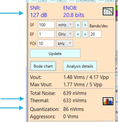
<Figure 23>
An updated thermal noise plot also tells this tale. Click on the Thermal Noise Bar Chart icon again, and notice a second thermal noise dialog pops up, in addition to the one we took a snap-shot of earlier.
NOTE: If the earlier window is hiding, you can hover of the SCE icon in the desktop’s task bar to find it and bring it into view. Do the same for the other. It may take some finagling to get them both showing where you want them.
You can arrange the two plots on the screen for comparison purposes. We show the two plots below, (where we’ve given the second plot a new title reflecting the change to 10,000 pF). Notice how the peak of the noise has shifted from 3.2 MHz to closer to 20 kHz. More importantly, the scales on the plots have changed (look at the left side vertical axis) from uVs to 10’s of nV’s.
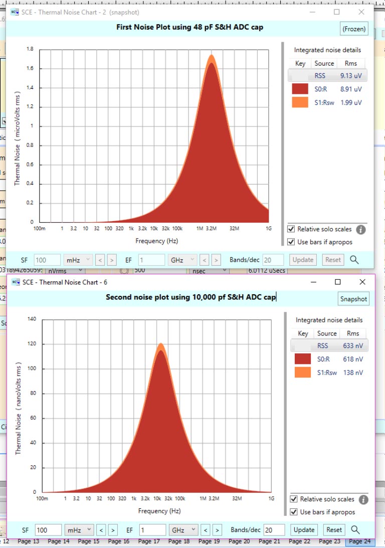
<Figure 24>
This shifting and reduction of noise is due entirely to the lower system corner. The quantization noise of our system is still what it was before — 86 nV due to the 24 bit ADC.
You can close all the plots for the next step, where you’ll get practice in adding a stage — in this case, an amplifier stage.
Step 10 – Adding, Disabling, and Removing Stages
In later steps, we’ll be showing you some of the basics of using a gain stage. But before we can do this, we need to show you how to add stages to the signal chain. You’ll also want to know how to disable a stage (for experimentation / comparison purposes) and finally, how to remove a stage altogether.
Stages are added by choosing one from the Stage Library Panel, which resides on the left side of the main screen. This panel may be collapsed / expanded using the chevron button in the upper left corner as you saw early in Step 8. Another way to open the panel is to click on one of the vertical tabs on the left border of the main window. This is also how you select a group of stages to choose from. The groups consist of sensors, series stages, shunt stages, voltage divider stages, amplifier stages, specialty stages, and a set of miscellaneous stages. You can practice by selecting each of these tabs in turn to see what stages are available.
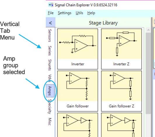
<Figure 25>
To add a stage to your signal chain, you double-click on its stage icon. But before you do, you need to understand where the stage will be inserted into the signal chain. The rule is this: The new stage will be added to the right of the currently selected stage. That stage can be determined by looking for cyan coloring at the bottom of the stage icon, and also by what stage definition is showing in the middle Stage Definition Panel.
Suppose we wish to add a voltage “gain follower” (non-inverting) amp stage right after the sensor stage. So first, ensure that the sensor stage is selected, and then select the Amps tab on the left hand side of the library panel, and then double-click on the Gain Follower Amp Stage icon. A new copy of this stage will be inserted right after the sensor stage, and then will automatically selected as the current stage.
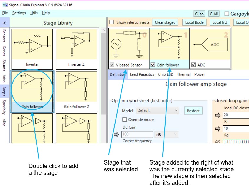
<Figure 26>
NOTE: If you instead had the ADC stage selected, then the amp stage would have been added in front of the ADC stage. The reason? You aren’t allowed to add a stage after an ADC stage, and so it puts the new stage where it can — as in … right before the ADC.
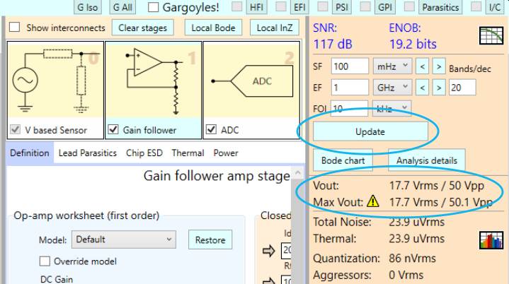
To see the effects of adding the amp stage, click the main Update button, and notice changes to SNR, ENOB, Vout, and Max Vout. By default, the gain follower stage has a gain of 10x, so you’ll see that Vout has jumped to 17.7 Vrms — 50 Vpp (remember, this is at the FOI of 10 kHz). You’ll also notice the Max Vout field goes to 50.1 Vpp, (which in this case occurs at DC). And notice the yellow triangle warning sign. The Max Vout of 50 Vpp is way beyond the range of the ADC, which was given a 5 Vpp full scale by default.
<Figure 27>
You can correct this problem by either choosing a new full scale value for the ADC (50 Vpp is most likely not reasonable, though), or by changing the sensor output. We’ll do the latter in a step later on.
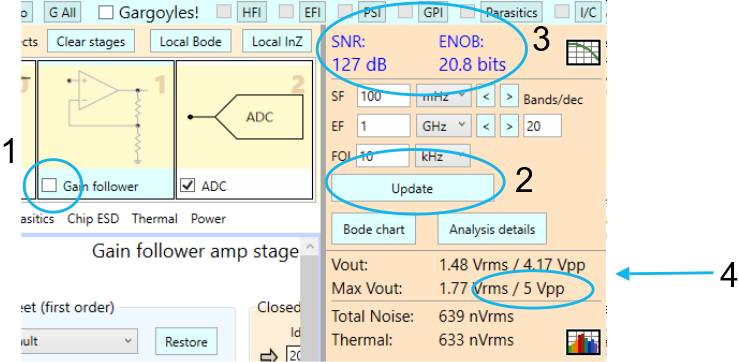
Suppose you want to go back and see what the output values were before you added the amp stage. You can do this by temporarily disabling the stage and then updating the analysis. This is accomplished by clicking on the Enable check box at the lower left corner of the stage icon. This check box acts as a toggle. Since the stage was enabled, it now becomes disabled. Once disabled, you can click the Update button to see the main system values change, and then perhaps click the Enable check box again to re-enable the amp stage, and the click Update again, and so on.
<Figure 28>
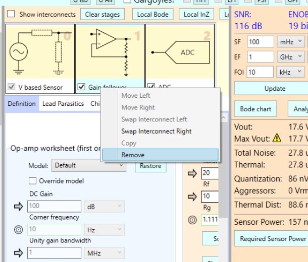
Suppose you wish to remove the new amp stage altogether. You can do this by using a right-mouse click on the stage icon. A menu pops up where you can select the Remove entry. This menu also allows you to move the stage left or right in the chain — that is, change the order of the stages — by using the same popup menu.
<Figure 29>
NOTE: If you try to move the amp stage left or right in this simple signal chain, you’ll find you can’t. In fact, the menu entries for this are grayed out on this stage. Why? Each signal chain MUST have a sensor stage as the first stage. And if a signal chain has an ADC stage (which is optional by the way), that stage MUST be the last stage in the chain. Thus, there’s no place to move the amp stage. It can only be in the middle.
Step 11 – Inspecting the Basic Properties of the Amp Stage
Let’s delve a little bit into the definition of our amp stage. First, ensure the amp stage is enabled, or if you removed the stage in the last step, add it back again.
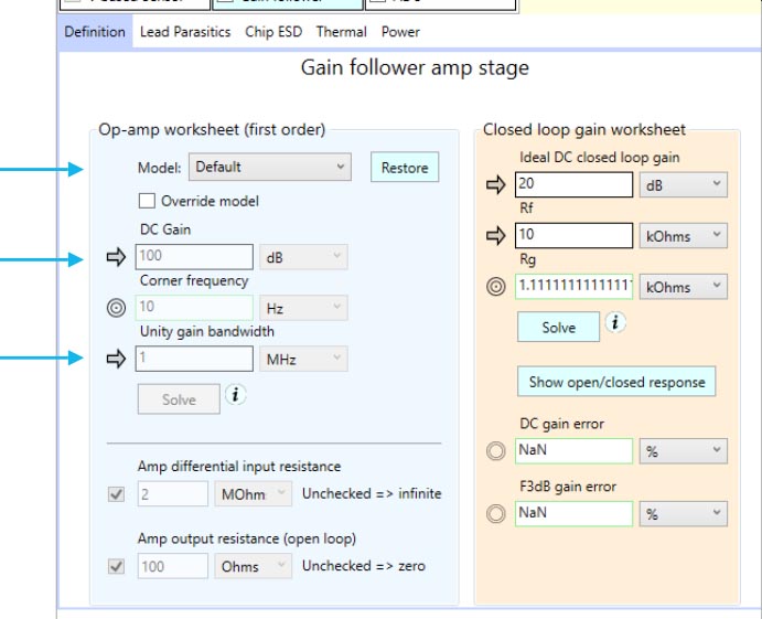
The stage definition for the Gain Follower should appear in the middle panel. Be sure to select the Definition tab if it’s not already selected. In the upper left Amp worksheet, you can choose from a set of pre-defined op-amps, and/or change parameters and define your own custom amp. Notice that the “Default” op-amp comes pre-selected. This amplifier has first-order properties similar to a 741-class op-amp. Notice the DC gain of around 100 dB, and Unity Gain Bandwidth of 1 MHz.
<Figure 30>
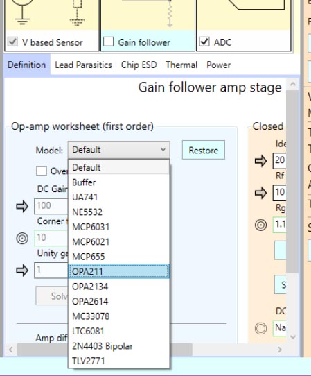
Let’s change to a different op-amp — in this case, the OPA211. You can do this by using the combo-box drop down at the top of the op-amp worksheet, and then selecting OPA211.
<Figure 31>
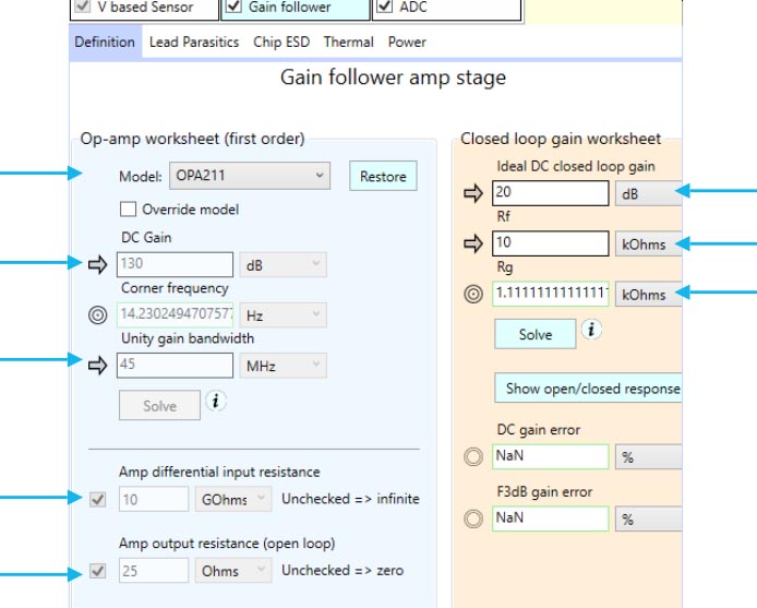
The worksheet will update after you’ve made your selection. From this worksheet, you can see the OPA211 has a DC Gain of 130 dB, a UGBW of 45 MHz, a high, 10 GOhm input resistance, and a fairly low 25 ohms of output resistance.
<Figure 32>
To the right of the amp worksheet is the Closed Loop Gain Worksheet. Here, you can set the values of the gain resistors to achieve whatever closed loop gain you want. The defaults here are 10 kOhms, and 1.1 kOhms, respectively, giving us 20 dB (10X) gain.
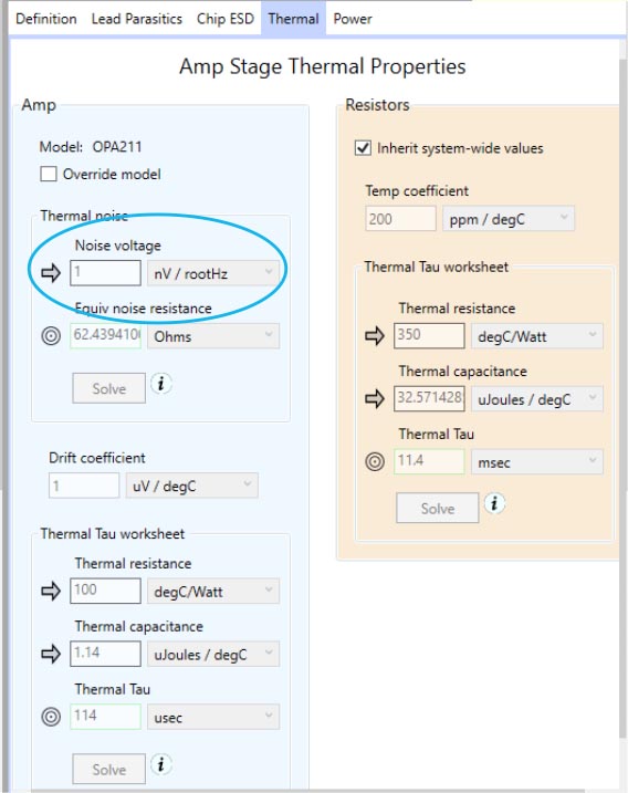
Next, let’s examine the thermal parameters assigned to the stage, which can be found by clicking on the horizontal Thermal Tab that appears at the top of the stage definition panel.
<Figure 33>
In our example, we see that the op-amp has thermal noise of 1 nV/rootHz, which is equivalent to roughly 62 ohms, as seen in the Amp’s thermal noise worksheet. There are two other worksheets in this panel, including one to determine the first-order “thermal tau” of the amplifier, used to help determine the voltage drift cause by heating of the amplifier, and also a panel to determine the temp-coefficients for the two main resistors of the stage (in the current product, they all get the same properties), as well as the thermal tau properties of said resistors.
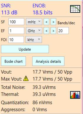
Our main concern for this lesson is the thermal noise. To see its effect on the overall system SNR, alternatively disable and enable the amp stage, while pressing the Update button to see the difference. You’ll see without the amp in the system, SNR and ENOB are 127 dB / 20.8 bits, with a thermal noise of 633 nVrms, and with the amp, as shown in the figure below, we have an SNR and ENOB of 113 dB / 18.5 bits, and a thermal noise of 39.3 uVrms.
<Figure 34>
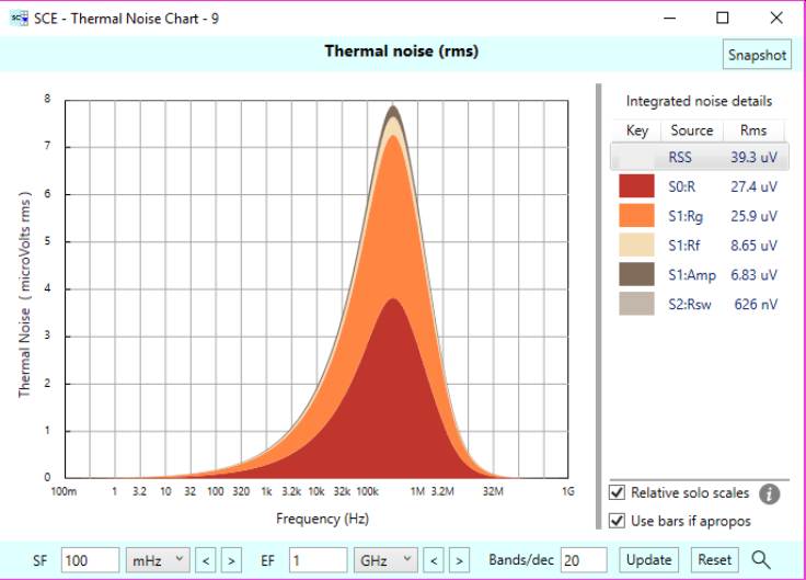
Why the large increase in noise when the amp stage is added? Besides the thermal noise generated by the amp itself (we saw that earlier: 1 nV/rootHz at the amp’s input) there is also noise generated by the two stage resistors Rf and Rg, which default to 10 KOhms and 1.11 KOhms. These end up contributing 8,65 uV and 25.9 uV of integrated rms noise, respectively. Notice that Rg (the resistor to ground) is the main culprit, even though its resistance is less. We’ll leave that mystery for another day, but for now, you may wish to popup the thermal noise chart at this point and see how these noise sources stack up.
<Figure 35>
A big part of signal chain design is optimizing the resistances to yield the best SNR possible. For an example of how this might be done, see the blog post Noise Distribution Considerations for a Multi-stage Audio Amplifier.
Step 12 – Adjusting the Sensor Voltage
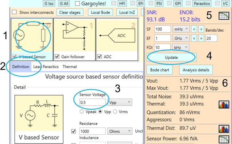
Because the Max Vout of 50 Vpp is way beyond the scale of our A/D, our signal chain isn’t properly constructed, so the values shown on the analysis panel aren’t very useful. That’s the reason you see the warning icon next to the Max Vout field. Because we added 10x gain with the amp stage, we should reduce the sensor voltage by the same amount, and then we’ll get back to a Max Vout of 5 Vpp. So do this now by selecting the source stage again, and changing the sensor voltage to 0.5 Vpp.
<Figure 36>
Step 13 – Inspecting Analysis Details
In this final step of Lesson 1, we’ll introduce you to the Analysis Details Dialog, which can be accessed using the Analysis Details button to the right of the Bode chart button in the main analysis panel.

<Figure 37>
The details dialogs lists each source of noise in the signal chain and its noise voltage. A noise summary is given at the beginning, which repeats some of the information that can be seen in the summary section of the Analysis Panel on the main screen, such as the overall thermal noise, quantization noise, and another curious source called Aggressor noise. This is the noise caused by gargoyles — interferers — in the system, which is the subject of Lesson 2.
Conclusion
You can see that SCE is chock full of features, and we’ve only scratched the surface! We do think, however, that once you are used to it, you’ll find you can quickly and easily explore the design parameters of a signal chain, perhaps learning many new things along the way. That is, after all, the main purpose of the product.
Now, onwards to Lesson 2! … Well, once we get it posted anyway.
Comments
SCE Lesson 1 – Building and Analyzing Your First Signal Chain — No Comments
HTML tags allowed in your comment: <a href="" title=""> <abbr title=""> <acronym title=""> <b> <blockquote cite=""> <cite> <code> <del datetime=""> <em> <i> <q cite=""> <s> <strike> <strong>