Understanding Effective Number of Bits
One of the main figures of merit computed by Signal Chain Explorer is the Effective Number of Bits (ENOB) of your signal chain. In this Short and Sweet article we’ll explain how that number is computed. The ENOB value relates the Signal to Noise Ratio (SNR) of a system in regards to digitized output. For example, if your system outputs 16-bit data words, how many of those bits are actually useful? The useful number of bits is called the effective number of bits, and is less than the ideal because of noise in the system.
Manufacturers of A/D converters (ADCs) use the ENOB number as one measure of the quality of their converters. While the ENOB term is usually associated with ADCs, it can also be used as a measure of an entire signal chain — not just the ADC. You’ll see how that’s done in this article. But first, let’s look at ADCs by themselves, starting with mythical ideal converters that have no errors, noise, or distortion other than that caused by the quantization itself.
Ideal ADC Resolution
There are many sources of errors that can occur in a converter: Thermal noise, harmonic distortion caused by non-linearity, jitter, interference, etc. But we’re going to focus on just one source: the quantization noise. In an ideal ADC, that’s the only noise it has — but note that it will have such noise. There’s no getting around it. It’s inherent in the process of digitization.
NOTE: In this article we’ll be discussing basic Nyquist-sampling ADCs, not the fancy over-sampling ADCs, including ones that purposely inject a small dither voltage into the input. These fancy ADCs can have less quantization noise than what’s discussed here.
Suppose you have an ADC that has a full scale input of FS Vpp and data word size of N bits. The converter does its best to break up that full scale range into equal-sized chunks called quanta. There are \(\displaystyle {{2}^{N}}\) levels possible in a N bit converter, and \(\displaystyle {{2}^{N}}\) quantas.
Mathematically, we write:
\(\displaystyle Numlevels={{2}^{N}}\)
\(\displaystyle Q=\frac{{FS}}{{{{2}^{N}}}}\quad \text{ }\!\!\{\!\!\text{ V }\!\!\}\!\!\text{ }\)
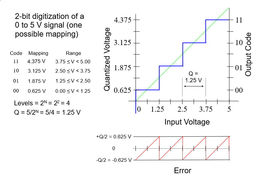
Here’s an example of the mapping in a lowly 2-bit converter with a 5 V full scale. We picked such a low resolution to emphasize the quantization errors that occur. The following figure shows one way that input voltages could get turned into digital output codes in this converter.

Our 2 bit ADC converter has \(\displaystyle {{2}^{N}}=4\) levels, and each quanta is 1/4= 1.25 V.
NOTE: The mapping we used in the figure is only one of the possible mappings. What mapping works best really depends on the needs of your application.
Quantization Error
We’ve chosen the code mapping so that a code of 00 corresponds to 0.625 V. But that code really represents all voltages in the range 0 <= X < 1.25. If the input voltage is 0 V, a 00 code will be output, but to the user of the digital data this code represents 0.625 V. So there’s a representation error of -0.625 V. If the input voltage happens to be 0.625 V, then a 00 code is again output, but there’s no error in the representation. After that, the error goes positive as the input voltage goes up. For example, if the input voltage is, say, 1.24 V, then the 00 code is still output, but now with an error of +0.615 V.
A transition occurs right at an input voltage of 1.25 V. Here the code output will change to a 01, which represents a voltage of 1.875 V. Now we have an error between what the input actually was (1.25 V), and what we represent it to be (1.875 V) of -0.625 V. The error is once again negative.
If the input voltage rises to 1.875 V, then the 01 code accurately represents the voltage, so there’s no error.
And so on, and so forth.
Quantization Noise
As we’ve seen, when a continuous voltage is digitized, there’s an error between what the input voltage is, and what the digital code assigned to it implies. The red line in the error plot of our previous figure shows how this error changes as we sweep the voltage range. Note that the error ranges from -Q/2 (-0.625 V) to +Q/2 (+0.625V).
It’s possible to find a statistical measure for this quantization error by using mean-square analysis. Without further ado, the derivation goes something like this:
\(\displaystyle {{Q}_{{noise}}}^{2}=\frac{1}{Q}\int\limits_{{-Q/2}}^{{+Q/2}}{{{{x}^{2}}dx}}=\left. {\frac{1}{Q}\frac{{{{x}^{3}}}}{3}} \right|_{{-Q/2}}^{{+Q/2}}=\frac{{{{{(Q/2)}}^{3}}}}{{3Q}}-\frac{{{{{(-Q/2)}}^{3}}}}{{3Q}}=\frac{{{{Q}^{2}}}}{{{{2}^{3}}3Q}}+\frac{{{{Q}^{2}}}}{{{{2}^{3}}3Q}}\)
\(\displaystyle {{Q}_{{noise}}}^{2}=\frac{{2{{Q}^{2}}}}{{24Q}}=\frac{{{{Q}^{2}}}}{{12}}\)
From this, we can write the formula for the quantization noise as:
\(\displaystyle {{Q}_{{noise}}}=\frac{Q}{{\sqrt{{12}}}}\quad \{Vrms\}\)
As noted in the formula, this is an RMS value — it is after all the root of a mean-square value. This noise is considered to be random, Gaussian white noise. It’s considered to be uncorrelated with the signal, so that’s why it’s considered random. And it’s assumed that any input voltage is equally likely, and thus any error in the range of errors is equally likely. But that’s not always the case — there could be interaction between signal frequencies and the sampling frequencies in the converter. However, in the absence of information to the contrary, treating the noise as being uncorrelated and random is reasonable.
Let’s write the noise in terms of the full scale voltage and the number of bits by plugging in the equation for quanta we gave earlier. We’ll use this form in a bit:
\(\displaystyle Qnoise=\frac{Q}{{\sqrt{{12}}}}=\frac{{FS}}{{\sqrt{{12}}({{2}^{N}})}}=\frac{{FS}}{{\sqrt{{4\times 3}}({{2}^{N}})}}=\frac{{FS}}{{2\sqrt{3}({{2}^{N}})}}\quad \{\text{Vrms }\!\!\}\!\!\text{ }\)
Signal to Noise Ratio of an Ideal ADC
The signal to noise ratio of a system is defined to be the RMS voltage of the signal divided by the RMS voltage of the system’s noise. For an ideal ADC, which has only quantization noise, we can write:
\(\displaystyle SNR=\frac{{Signa{{l}_{{rms}}}}}{{Nois{{e}_{{rms}}}}}=\frac{{F{{S}_{{rms}}}}}{{Qnoise}}\)
Both terms are RMS voltages, making the ratio unit-less. Since FS is really a peak-to-peak voltage, we must convert it into RMS as follows:
\(\displaystyle F{{S}_{{rms}}}=\frac{{FS}}{{2\sqrt{2}}}\)
Using our definitions for FSrms and Qnoise we can derive:
\(\require{cancel} \displaystyle SNR=\frac{{F{{S}_{{rms}}}}}{{Qnoise}}=\frac{{\cancel{{FS}}}}{{\cancel{2}\sqrt{2}}}\times \frac{{\cancel{2}\sqrt{3}({{2}^{N}})}}{{\cancel{{FS}}}}=\frac{{\sqrt{3}({{2}^{N}})}}{{\sqrt{2}}}={{2}^{N}}\sqrt{{{3}/{2}\;}}\)
In dB:
\(\displaystyle SN{{R}_{{dB}}}=20Log10({{2}^{N}}\sqrt{{{3}/{2}\;}})=20Log10({{2}^{N}})+\,20Log10(\sqrt{{{3}/{2}\;}})\)
\(\displaystyle SN{{R}_{{dB}}}=20Log10(2)N+20Log10(\sqrt{{3/2}})\)
\(\displaystyle SN{{R}_{{dB}}}\approx 6.02N+1.76\)
Effective Number of Bits
Next we’ll consider real-world, non-ideal converters. In the real world, the converters have more than just quantization noise. They have thermal noise, clock jitter noise, non-linearities that cause distortion, outside interference, etc. In the absence of information to the contrary, it’s useful to treat all this noise as uncorrelated, random noise. As such, this noise can be root-sum-squared along with quantization noise to produce the overall RMS noise of the converter:
\(\displaystyle {{N}_{{overall}}}=\sqrt{{Qnois{{e}^{2}}+{{N}_{1}}^{2}+{{N}_{2}}^{2}+…+{{N}_{n}}^{2}}}\quad \{Vrms\}\)
If we replace the Qnoise term in the denominator of our SNR with this overall noise, we end up with what’s called the Signal-to-Noise-And-Distortion (SINAD) ratio:
\(\displaystyle SINAD=\frac{{F{{S}_{{rms}}}}}{{{{N}_{{overall}}}}}\)
Now, suppose we take the equation that relates SNR with N bits, and replace the SNR term with SINAD instead. We can solve for N, and this N is then called the Effective Number of Bits (ENOB) of the converter. For example, using the dB version of the SNR equation we can write:
\(\displaystyle \begin{array}{l}SN{{R}_{{dB}}}=20Log10(2)N+20Log10(\sqrt{{3/2}})\quad \quad \quad \quad \{\text{original equation }\!\!\}\!\!\text{ }\\SINA{{D}_{{dB}}}=20Log10(2)ENOB+20Log10(\sqrt{{3/2}})\quad \{\text{SINAD version }\!\!\}\!\!\text{ }\end{array}\)
Solving for ENOB yields:
\(\displaystyle ENOB=\frac{{SINA{{D}_{{dB}}}-20Log10(\sqrt{{3/2}})}}{{20Log10(2)}}\approx \frac{{SINA{{D}_{{dB}}}-1.76}}{{6.02}}\)
For a given real-world ADC having an N-bit output data width, the ENOB of that converter will be less than N because it will have noise above and beyond the quantization noise. A 16-bit ADC, for example, may actually have an ENOB of 14 bits.
How is ENOB found for a particular device? The steps might be something like the following, for which we will not go into detail (and note there are other ways to determine ENOB):
- A known signal is input to the device under test.
- The digital output data of the converter is processed through an FFT, and the frequency spectrum is analyzed. A measure of the strength of the signal is found, along with a measure of the noise. In a real world device, this noise is made up not only of quantization noise, but also thermal noise, harmonic distortion, intermodulation distortion, sampling jitter, etc.
- Given the signal and noise measurements, the Signal-to-Noise-and-Distortion (SINAD) ratio of the device can be computed.
- The SINAD term can be used to back-calculate the ENOB.
The following figure illustrates the determination of the signal and noise relationship:

Philosophy of finding ENOB for an entire signal chain
It’s useful to step back and look at the big picture about the implications of using the ENOB formula. We are in effect (pun intended) taking a real world ADC and mapping it to a mythical, ideal ADC. Remember that an ideal ADC has only quantization noise. By using the ENOB formula on our real world ADC, we are pretending that the corresponding, mythical, ideal ADC has quantization noise that just happens to equal the total noise of our real-world ADC. That is,
\(\displaystyle \text{Mythical Ideal }{{Q}_{{noise}}}=\text{Total Real Worl}{{\text{d}}_{{noise}}}\)
If we were to use either device, mythical or real, the quality of their digital outputs would be the same, in terms of useful bits.
This method of determining ENOB can also be applied to an entire signal chain that includes an ADC at the end. Think about it: We have a given input signal, we can look at the digital output of the whole chain, measure the corresponding noise, compute the corresponding SINAD, and find the effective number of bits. It’s as though we’ve packaged up that entire signal chain and placed it inside a black box.

As far as anyone on the outside is concerned, that black box serves exactly the same function that an ADC does: It takes an analog input signal and outputs digital values.
It should be noted that an ADC chip itself is more than just a collection of comparators. It’s a complicated affair, involving much circuitry. Why, that circuitry is exactly like a signal chain!
Signal Chain Explorer uses the above philosophy when computing ENOB for you. By reporting the ENOB, it’s telling you what mythical, ideal, ADC device your signal chain is equivalent to, in terms of output quality.
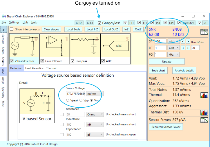
Let’s see this in action. Below is a signal chain involving a sensor, an amplifier, a low-pass filter, and an ADC at the end of the chain. Each of these stages contributes noise. In the example here, that noise includes thermal noise in the resistors and amplifiers of the various stages, as well as noise from external interferers, (which we call gargoyles). In this case, the gargoyles are a microprocessor clock line that’s placed too close to the signal line, causing electrical and electromagnetic interference, as well as a switching power supply also causing interference, and also causing ground plane interference.
NOTE: We aren’t showing the gargoyles in detail below. Only that they are turned on.

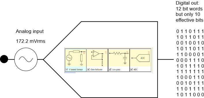
Signal Chain Explorer is reporting an ENOB of 10 bits corresponding to an SNR (really SINAD) of 62 dB. This is for an input voltage in the sensor of 172.2 mVrms. So our signal chain looks like a mythical ADC that has 10 effective bits of resolution, and a full-scale voltage of 172.2 mVrms:

Note that the ADC of the signal chain itself actually has an ideal resolution of 12 bits, (definition not shown), so we see how noise in the whole system degrades that ideal — from 12 bits down to 10 bits. 12-bit data words are pumped out, but on average, only 10 bits of each word has useful information.
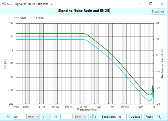
The ENOB we just showed was for a frequency of interest (FOI) of 1 kHz. The effective number of bits actually varies with frequency, (because both the noise and signal are affected by amplifier roll-off, low pass filter roll-off, etc.), and we can see the variations by pulling up the ENOB plot in SCE. That plot shows ENOB along with the SNR (really SINAD) of the signal chain:

Comments
Understanding Effective Number of Bits — No Comments
HTML tags allowed in your comment: <a href="" title=""> <abbr title=""> <acronym title=""> <b> <blockquote cite=""> <cite> <code> <del datetime=""> <em> <i> <q cite=""> <s> <strike> <strong>